By Mark LaPedus
The 2nm process race is off and running, as several chipmakers are scrambling to develop and ship this next-generation technology.
At this week’s 2024 IEEE International Electron Devices Meeting (IEDM) in San Francisco, TSMC described more details about its 2nm process. In addition, Samsung recently outlined its 2nm process. And Intel is working on a more advanced version of the technology.
Clearly, TSMC won the 3nm process race. Right now, though, it’s difficult to say which vendor is leading the 2nm race. Each vendor is in various stages of development. So where does each vendor stand right now?
TSMC
TSMC, the world’s largest foundry vendor, offers a range of processes, ranging from mature to advanced technologies. The company’s most advanced process is based on a “3nm” technology. TSMC’s 3nm process incorporates tiny transistor structures called finFETs.
Transistors, one of the key building blocks in chips, are tiny structures that act like electronic switches in devices. Today’s advanced chips have billions of tiny transistors.
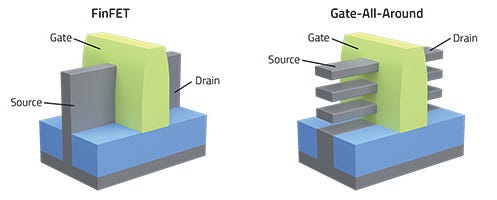
But the workhorse finFET transistor has finally run out of steam and reached its physical limits. So, starting at the 2nm node (N2) in 2025, TSMC will migrate to a new transistor type called the nanosheet FET. It’s also known as a gate-all-around (GAA) transistor. Nanosheet FETs provide better performance than finFETs, but they are harder and more expensive to make in the fab.
FinFET vs Gate-all-around or nanosheet FET Source: Lam Research
For some time, TSMC has been talking about its 2nm process. At this week’s IEDM, TSMC presented more details about the technology. “This industry-leading N2 logic technology features energy-efficient gate-all-around nanosheet transistors, middle-of-line and backend-of-line interconnects with the densest SRAM macro of ~38Mb/mm2. N2 delivers a full node benefit from the previous 3nm node in offering a 15% speed gain or a 30% power reduction with a >1.15x chip density increase,” said Geoffrey Yeap, vice president of advanced R&D technology at TSMC, in the IEDM paper. Others contributed to the work.
The process features a near-ideal 60.1mV/dec sub-threshold swing with six-Vt offerings spanning across 200mV. TSMC’s N2 NanoFlex standard cell architecture enables nanosheet width modulation.
For the metal layers, TSMC’s 2nm process will incorporate traditional copper interconnects. The company won’t move to a backside power delivery network until the next nodes.
The 2nm process features a barrier-less all-tungsten middle-of-line (MoL) layer. “Optimized M1 with novel 1P1E EUV patterning led to close to 10% std cell capacitance reduction and a savings of multiple EUV masks,” Yeap said. “In summary, N2 MoL and BEOL RC are reduced by ~>20%, contributing significantly to energy-efficient compute.”
Currently in risk production, TSMC’s N2 platform technology is scheduled for mass production in the second half of 2025. Another TSMC process, dubbed N2P, is in the works. N2P is a 5% speed enhanced version of N2 with full GDS compatibility. It is expected to complete the qualification stage in 2025 with mass production slated for 2026.
Samsung
In 2022, Samsung began shipping chips based on nanosheet FETs at the 3nm node. Samsung took the lead in the nanosheet market. But the company continues to struggle with its yields here.
Samsung recently shipped its second-generation 3nm nanosheet FET technology. In a scanning electron microscope (SEM), TechInsights found Samsung’s new 3nm nanosheets within the company’s Exynos W1000 processor. The processor is believed to be incorporated in Samsung’s smartwatch.
“The gate-level die photograph further illustrates the processor's core components: a high-performance single-core Arm Cortex-A78 CPU, a high-efficiency quad-core Arm Cortex-A55 CPU, and a dual-core Arm Mali-G68 GPU,” according to TechInsights in a blog.
Like TSMC, Samsung hopes to ship its 2nm nanosheet technology in 2025. Samsung refers to its 2nm technology as SF2. “For GAA, Samsung Foundry will provide a highly advanced SF2 technology that offers significant improvements in performance, power, and area over SF3 GAA,” according to Samsung. “In addition, Samsung Foundry is accelerating the development of the SF2P process to meet the steadily growing demand for superfast computing. To reduce area even further, the Extreme High Density (xHD) library is enabled in SF2, lowering area in comparison to the HD library.”
Intel
Intel recently revised its chip-manufacturing roadmap. Previously, Intel intended to manufacture chips based on the following nodes—7nm, 4nm, 3nm, 20A and 18A. 7nm and 4nm are in production at Intel. The company has outsourced most of its 3nm chip production to TSMC.
Intel had big plans for its 20A process, which is based on nanosheet FETs. However, Intel recently scrapped the 20A process and decided to move directly to its 18A technology.
Originally, Intel was supposed to manufacture its Arrow Lake processor family at the 20A node. Now, Intel’s Arrow Lake processor family is built by TSMC and packaged by Intel.
Intel is moving full speed ahead to manufacture its 18A process within its own fabs. Slated for 2025, Intel’s 18A consists of two new technologies—the RibbonFET gate-all-around transistor architecture and the PowerVia backside power delivery technology.
(Send comments to: mdlapedus@gmail.com Semiecosystem reserves the right to post and edit comments.)


