
5 Takeaways From Intel’s Foundry Event
New processes, packages and alliances were among the hot topics

By Mark LaPedus
At its foundry conference in San Jose, Calif., Intel made several new announcements and updated its foundry process roadmap.
As part of the announcements, Intel reiterated that its next-generation 18A process is on track for delivery in the second half of 2025. But at the event, Intel also made a somewhat surprising disclosure about 18A, a process that is supposed to give the company a competitive edge in the leading-edge foundry business.
Intel disclosed that 18A is mainly targeted for a narrow set of high-performance applications. In other words, 18A isn’t exactly a “mainstream” offering for foundry customers.
At the event, Intel unveiled a more mainstream version of 18A. That process, called 18A-P, is a derivative of 18A. Targeted for 2026, 18A-P is designed for a broader set of foundry customers. So it appears that Intel’s foundry unit will push 18A-P for high-end mainstream foundry applications.
In addition, Intel introduced new advanced packages, a chiplet alliance and other technologies at the event.
Intel’s event, called Intel Foundry Direct Connect, was held on April 29 in San Jose. The event brought together more than 1,000 attendees. I attended the conference and here are my five takeaways from the event:
1-Can Intel turn the foundry business around?
Lip-Bu Tan, the new chief executive of Intel, faces several challenges. Among them are:
*Intel needs to speed up the development of its x86-based processor lines for the server market. The company is losing ground here.
*The company needs a new AI chip strategy. Its previous efforts in AI have fallen short.
*It must address its loss-ridden foundry business.
In 2010, Intel entered the foundry business. But the company was unable to gain any traction, causing it to exit the business a year or two later.
Then, in 2021, Intel reentered the foundry business. At the time, the company announced plans to develop five processes in four years. The goal was to regain the leadership position in process technology. In addition, Intel also announced several new fab projects.
Foundry customers applauded Intel’s ambitious plans. Customers want more choices in terms of leading-edge foundry processes.
To date, though, Intel has struggled to gain any noticeable traction in the foundry business. Some fab projects have been delayed. And it continues to lose money in the business.
Intel is working with several foundry customers, including Amazon, MediaTek, Microsoft and the U.S. Department of Defense (DoD). Nvidia is also a possible customer. But the vast majority of Intel’s foundry sales come from the company’s own product groups. That won’t change anytime soon.
So, the questions are clear: Will Intel ever become successful in the foundry business? If so, how?
Intel is taking several steps to turn its foundry business around, including:
*It is in the process of turning its foundry unit into an independent subsidiary. That will give the foundry unit more autonomy, enabling it to make faster decisions.
*The company is expanding its process roadmap (see below for details). That will give foundry customers new and different process options.
*It is expanding its packaging technology offerings. That’s an area where Intel is having success.
“Intel is committed to building a world-class foundry that serves the growing need for leading-edge process technology, advanced packaging and manufacturing,” said Tan. “Our No. 1 job is to listen to our customers and earn their trust by creating solutions to enable their success. The work we are doing to drive an engineering-first culture across Intel while strengthening our partnerships throughout the foundry ecosystem will help us to advance our strategy, improve our execution and win in the market long term.”
That’s a good start. But is it enough? Intel still faces several challenges. It needs to find some high-volume foundry customers. And it needs to start making some money in the business.
2-Mature processes
At the event, Intel updated its foundry process roadmap, which can be split into two segments: mature and advanced processes.
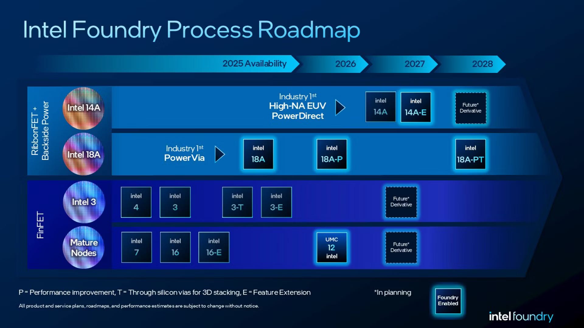
Intel’s foundry roadmap Source: Intel
Advanced processes tend to grab the headlines, but mature technologies are also important. Mature processes are used to make chips for a wide range of applications, such as automotive, consumer and industrial.
In the mature process segment, Intel is working on several technologies, including 16nm and 12nm.
*16nm. Intel is readying a 16nm foundry process, which is based on finFET transistors. One customer, MediaTek, is taping out its first chips based on Intel’s 16nm process.
*12nm. For some time, Intel and UMC have been working on a 12nm finFET foundry process. The process is due out in 2026 or so. Intel and UMC are also working on new 12nm derivatives.
3-Advanced processes-3nm, 18A
*3nm. Originally, Intel was supposed to manufacture its own processor lines based on its 3nm process. Intel’s 3nm process is based on finFET transistors. This is Intel’s first node using extreme ultraviolet (EUV) lithography.
But as it turned out, Intel ended up outsourcing most, if not all, of its 3nm production to TSMC. Now, Intel is trying to offer its 3nm process for foundry customers. That might be a hard sell.
*18A. For some time, Intel has been talking about its next-generation 18A technology. 18A combines a gate-all-around (GAA) transistor architecture with a backside power delivery technology. Compared to 3nm, 18A provides a 15% or more increase in performance and 1.3x in chip density. (Intel refers to its GAA transistor technology as the RibbonFET. Intel refers to its backside power delivery technology as the PowerVia.)
In the second half of 2025, Intel hopes to ship its first processor line based on its 18A process. This processor is codenamed Panther Lake.
Intel also hoped to win some foundry business with 18A. That may not happen as planned. When Intel was defining its 18A process several years ago, the company had only one customer in mind—Intel. At the time, Intel would use the process to develop new and faster chips.
Fast forward. When it recently began to discuss 18A with potential foundry customers, Intel discovered that the technology would only serve a narrow base of high-end applications. So 18A is still on track for the second half of 2025. Intel will use the process to manufacture its processor lines. It’s unclear if foundry customers will use it.
*18A-P. 18A-P, a variant of 18A, is designed for a broader set of foundry customers. In other words, 18A-P is more of a mainstream foundry process. Compared 18A, 18A-P provides an 8% increase in performance and 1.0x in chip density. It has wide range of Vt levels and so on.
Intel will put more emphasis on 18A-P for mainstream leading-edge foundry customers. Early wafers based on 18A-P are in the fab now. 18A-P will be design rule-compatible with Intel 18A. 18A-P is expected to be released in 2026.
So given that time schedule, Intel’s hopes to gain traction in the foundry business might be delayed again. That still remains unclear.
*18A-PT. This is another new variant that builds on Intel’s 18A-P process. 18A-PT is due out in 2028.
4-Future processes—14A, 14A-E
*14A. 14A represents Intel’s second-generation RibbonFET and PowerVia technologies. Compared to 18A, 14A provides a 15%-20% increase in performance, a 25%-35% reduction in power and 1.3x in chip density.
14A is due out in 2027. 14A-E, which is also due out in 2027 or so, is an enhanced version of 14A.
5-New packaging technologies
At its event, Intel introduced several new advanced packaging offerings, including:
*Foveros-R. This features a redistribution layer (RDL) interposer, which in turn creates heterogeneous integration between chiplets. Foveros-R is expected to be ready by 2027.
*Foveros-B. This combines RDLs for power and signal with silicon bridges to provide advanced packaging solutions for complex designs. Foveros-B is due out in 2027.
*EMIB-T. Several years ago, Intel introduced EMIB, an embedded bridge technology for advanced 2.5D packages. EMIB-T adds through-silicon vias (TSVs) to the bridge.
Foveros-R and Foveros-B appear to compete against TSMC’s Chip on Wafer on Substrate (CoWoS) technology. CoWoS is used to assemble and stack several chips in the same package. CoWoS is what many call a 2.5D package.
At present, there is a shortage of CoWoS capacity in the market. Perhaps that’s a new opportunity for Intel.
Here are other announcements at the event:
*Intel formed two new ecosystem programs--Intel Foundry Chiplet Alliance and the Value Chain Alliance (VCA). The Chiplet Alliance focuses on optimizing the ecosystem for chiplets. The VCA are partners that provide ASIC and SOC design services.
*Intel formed an alliance with Amkor Technology. Amkor will provide assembly services for Intel’s EMIB technology.