
5 Takeaways From TSMC’s Ecosystem Conference
Leading-edge processes, packaging, chiplets and RISC-V were among the highlights

By Mark LaPedus
TSMC recently held its Open Innovation Platform (OIP) Ecosystem Forum, a large conference that brings together TSMC, EDA companies, IP houses and test/assembly vendors.
The one-day conference featured a keynote session and multi-track presentations on various technologies. The idea behind the event is to get an update on TSMC’s process technology and packaging roadmaps. At the same time, several EDA vendors are developing design flows for TSMC’s processes. At TSMC’s event, the goal is to get an update on these design flows.
I attended TSMC’s recent North America OIP Ecosystem Forum, which was located in Santa Clara, Calif. (TSMC also holds the event in other parts of the world.) Here are my five takeaways from the conference:
*TSMC’s roadmap on track
*Huge demand for CoWoS
*TSMC’s panel-level packaging efforts
*Chiplets to the rescue
*Alphawave Semi, Andes roll out new products
I have described each takeaway in detail below.
TSMC’s roadmap on track
At the event, Taiwan’s TSMC, the world’s largest foundry vendor, provided an update on its advanced process technology roadmap. As expected, the roadmap is on track. There are no major changes here, as compared to the previous roadmap. TSMC, however, added a new 3nm derivative to the mix.
Before describing the roadmap, let’s briefly look at TSMC and its business model. First, TSMC is a pure-play foundry vendor. The company doesn’t design or sell its own chips. Instead, it manufactures a wide variety of chips for other companies in large facilities called fabs. Today, a leading-edge fab can cost around $20 billion—each.
TSMC’s foundry customers include AMD, Apple, Broadcom, Google, Intel, MediaTek, Nvidia, Qualcomm, Tesla and many others. In the foundry market, TSMC competes against Intel, GlobalFoundries, Samsung, SMIC, UMC and others.
Basically, in the foundry model, a company designs a chip line for a specific application. The chip design is then synthesized into a file format. Then, the company will hand off the chip design to TSMC (or another foundry vendor), which in turn will manufacture the chip line based on the specifications of the design.
Foundry vendors manufacture chips using various process technologies. A process is the recipe used to manufacture a given chip line.
TSMC offers both trailing- and leading-edge processes for foundry customers. Using these processes, TSMC and other foundry vendors can manufacture a wide variety of chips. Each chip incorporates an assortment of building blocks. Transistors, one of the key building blocks in chips, are tiny structures that act like electronic switches in chips. Today’s advanced chips have billions of tiny transistors in a single device.
Nonetheless, TSMC’s advanced process technology roadmap is split into two different transistor types—finFETs and nanosheet field-effect transistors (FETs). A nanosheet FET is sometimes referred to as a gate-all-around (GAA) transistor. The finFET represents the current technology. The nanosheet FET, or GAA, is the next-generation technology.
In any case, TSMC’s foundry customers have the option to have their chips built around finFETs or nanosheet FETs--or both. This depends on the application.
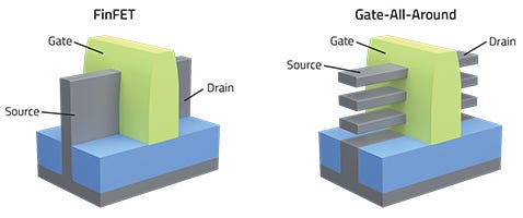
FinFET vs Gate-All-Around (or nanosheet FET) transistors Source: Lam Research
FinFETs aren’t new. Since 2013, TSMC has been manufacturing a wide variety of high-performance chips built around Fin Field Effect Transistors (FinFETs or finFETs). Right now, TSMC’s most advanced finFET process is based on the so-called “3nm” technology node. The company also makes chips using older finFET processes (i.e. 4nm, 5nm, 7nm, 12nm, 16nm).
For the foreseeable future, TSMC will continue to make chips using various finFET processes. Many applications will continue to use finFET-based chips.
In addition, TSMC and many other foundry vendors will continue to make chips at more mature, or trailing-edge, nodes, which involves processes at the 22nm node and above. There are still many applications for these types of chips, which include analog devices, CMOS image sensors, display ICs, MEMS, microcontrollers and RF products.
At the leading edge, meanwhile, the semiconductor industry is in the middle of a major transition. It is moving from one transistor type to a new technology.
Today, as stated, TSMC’s 3nm finFET process represents the company’s most advanced technology. But beyond the 3nm node, the workhorse finFET transistor has reached its physical limits. So, to enable next-generation chips, the semiconductor industry needs a new transistor type.
That’s where the nanosheet FET fits in. The nanosheet FET is a next-generation transistor, which is supposed to provide better performance at lower power than finFETs. With the nanosheet FET, the semiconductor industry will be able to move forward and develop the next wave of leading-edge chips for the foreseeable future.
The nanosheet FET falls under a class of transistor types called GAA. GAA-based transistors like nanosheet FETs have several advantages over finFETs, but they are harder and more expensive to manufacture in the fab.
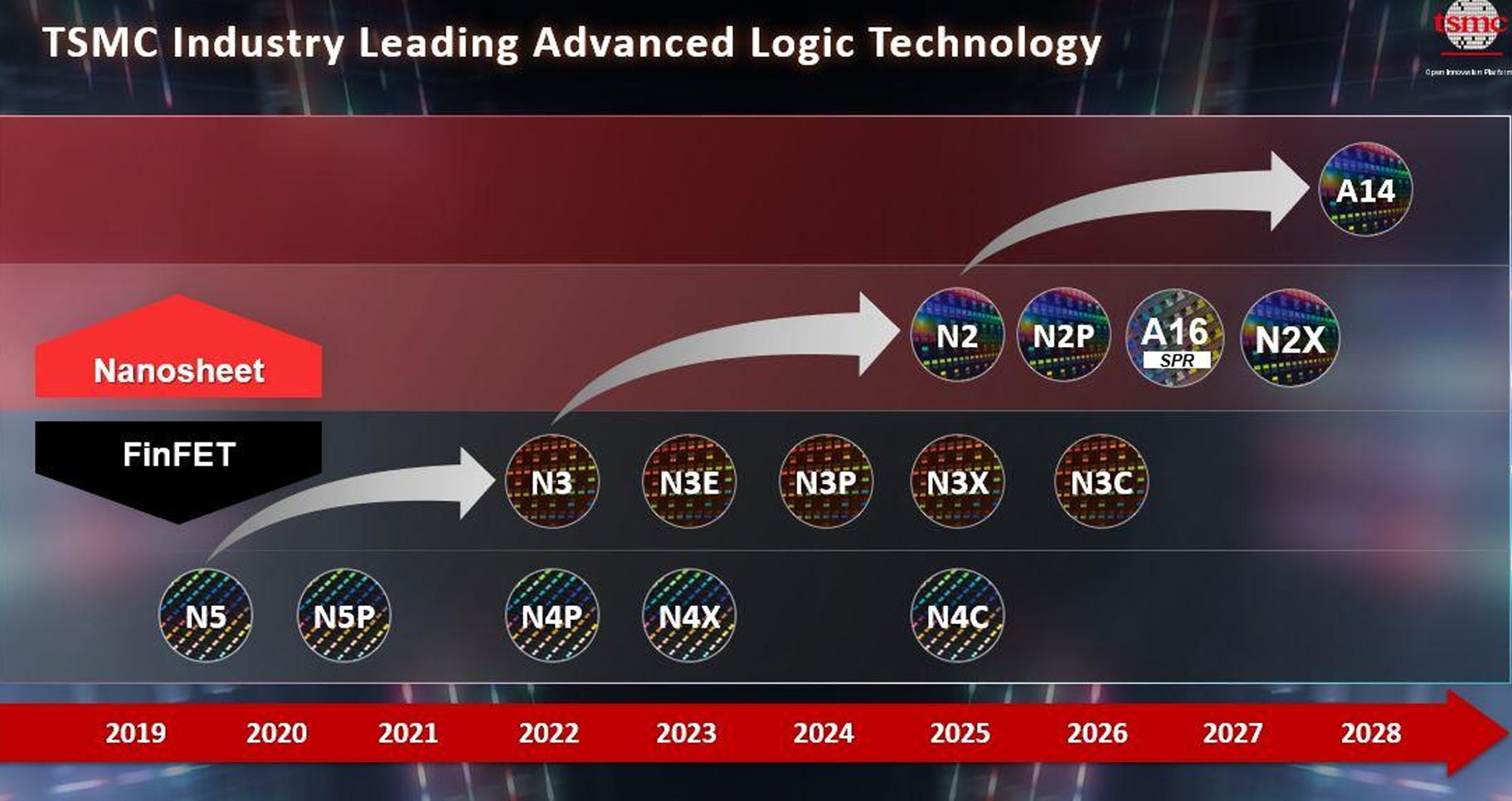
Meanwhile, later this year, TSMC will start making its first chips using nanosheet FETs at the 2nm node. TSMC refers to the 2nm node as N2. Nonetheless, here is TSMC’s advanced technology roadmap:
So, what does this all mean? Here’s a brief explanation:
Year--2025
N4C—An updated version of TSMC’s 4nm finFET process.
N3X—An updated version of TSMC’s 3nm finFET process.
N2—N2 represents TSMC’s new 2nm process. N2 is also TSMC’s first nanosheet FET technology. Compared to its 3nm process, N2 offers a 10%-15% speed improvement at the same power, or a 25%-30% power improvement at the same speed, and more than a 15% chip density increase.
Year--2026
N3C--TSMC added this process to the roadmap. It’s an updated version of TSMC’s 3nm finFET process.
N2P--A speed enhanced version of N2. N2P is a nanosheet FET technology.
A16—A16 is a nanosheet FET technology. A16 will incorporate TSMC’s new backside power delivery technology, dubbed Super Power Rail (SPR). Compared to N2P, A16 provides an 8%-10% speed improvement at the same power, or a 15%-20% power improvement at the same speed, and an additional 7%-10% chip density gain.
Year--2027
N2X—An updated version of TSMC’s N2 nanosheet process.
Year—2028
A14—A14 is TSMC’s second-generation nanosheet technology. Compared to N2, A14 offers a 10%-15% speed improvement at the same power, or up to a 30% power reduction at the same speed, along with more than a 20% increase in density. The initial A14 process does not include SPR. A14 with SPR technology is planned for 2029.
Huge demand for CoWoS
TSMC is experiencing huge demand for its foundry services, particularly in the high-performance computing (HPC) market. HPC involves AI chips, processors and other high-end devices.
The company is also experiencing enormous demand for its packaging services. In fact, it is scrambling to keep up with the demand for one packaging type called Chip-on-Wafer-on-Substrate (CoWoS).
IC-packaging is an important part of the semiconductor industry. In a semiconductor flow, a company designs a new chip line. Then, a chipmaker (i.e. TSMC, others) manufactures the chip line in a fab.
From there, the chips are sent to a separate facility, where they are assembled into an IC package. Basically, a chip resides inside a package. A package is a small enclosure that encapsulates and protects the chip from harsh operating conditions.
Generally, leading-edge chips are assembled into advanced packages. Advanced packages are used to help boost the performance of a given chip line.
TSMC offers different types of advanced packages for customers (See image below).
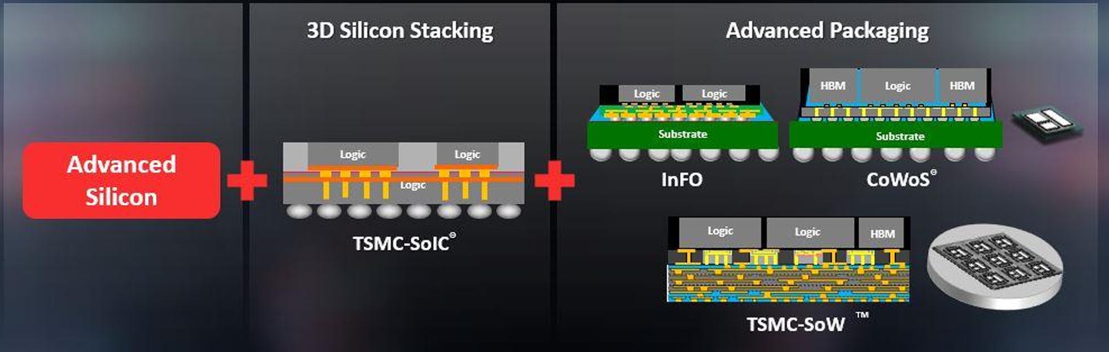
TSMC’s advanced packaging offerings Source: Company
TSMC’s CoWoS technology is especially noteworthy. CoWoS is used to assemble several different and complex dies all in the same package. In CoWoS, the chips are placed side-by-side on an interposer in the package. The interposer electrically connects the different dies. CoWoS is what many call a 2.5D package.
Meanwhile, AMD, Broadcom and Nvidia are experiencing huge demand for their respective AI chips in the market. Many of these AI chips are manufactured by TSMC. TSMC also packages these devices using its CoWoS technology.
Thanks to AI, TSMC is experiencing enormous demand for both its fab and CoWoS manufacturing capacity. TSMC is struggling to keep up with the capacity demands for CoWoS.
Take Nvidia (stock symbol “NVDA”) for example. “NVDA is now revising up its CoWoS demand modestly this year to 370K interposers, which represents over 90% growth, and for next year, has revised up its CoWoS supply to 530K interposers, which is 10% higher than its prior capacity and over a 40% increase over 2025,” said John Vinh, an analyst with KeyBanc Capital Markets, in a research note.
In addition, Broadcom (stock symbol “AVGO”) also wants more CoWoS manufacturing capacity from TSMC. For some time, Google has been designing and using its own AI chip, dubbed the Tensor Processing Unit (TPU). TPUs are incorporated into servers, which reside in Google’s data centers. Google works with Broadcom to design the TPU. The TPU is manufactured and packaged by TSMC. Broadcom also manages manufacturing processes for Google’s TPU.
For the next-generation TPU device, though, Google is apparently working with MediaTek. Meanwhile, Apple, OpenAI and others are co-developing AI chips with Broadcom.
“AVGO is significantly revising its CoWoS supply in 2026 to 190K, which represents over a 160% year-over-year increase, which is being driven by: 1) TPU strength as AVGO will have 100% share of TPU through 2026 given the delay of TPU7e (MTK); 2) TPU volumes are expected to double in 2026 as Google expects to broaden out the use of its TPU for AI workloads with external customers; and 3) the ramp of new AI ASIC wins at OpenAI (400-500K) and AAPL (100K),” Vinh said.
TSMC’s panel-level packaging efforts
In R&D, TSMC is quietly working on a new packaging technology, dubbed CoPoS or Chip-on-Panel-on-Substrate, according to various reports.
TSMC didn’t discuss CoPoS at its recent conference. But according to reports, CoPoS involves a panel-level packaging (PLP) technology.
PLP is a different way to manufacture advanced packages. Typically, in some advanced package types, multiple chips are processed and packaged on round 200mm or 300mm wafers. In PLP, though, multiple chips are packaged on a large rectangular substrate or a panel. PLP allows for more chips to be processed at the same time, thereby increasing the throughput. PLP also reduces manufacturing costs.
PLP isn’t new. For some time, ASE, PTI, Samsung, STMicroelectronics and others have been making packages using PLP.
In 2026, TSMC is expected to enter the PLP arena. Initially, the foundry giant will use a 310mm x 310mm panel. TSMC’s PLP efforts are worth watching. SemiVision, a technology site, has written about TSMC’s CoPoS technology in detail.
Chiplets to the rescue
At TSMC’s event, Kaushik Veeraraghavan, a software engineer at Meta, gave a keynote address on the latest trends in AI.
Meta, once known as Facebook, is a social media company. Meta processes and distributes an enormous amount of data within its own data centers. A data center is a large facility, which consists of a multitude of computers, networking infrastructure, cooling systems and other components. These computers, called servers, are equipped with AI chips, memory and other devices from various chip vendors.
Meta is also designing its own AI chip. Plus, the company recently acquired Rivos, a developer of AI chips, according to reports.
Meta and other companies face several challenges in developing high-end AI chips. Traditionally, for high-end applications like AI, chip vendors have developed complex devices, such ASICs or system-on-a-chip (SoC) designs. Generally, ASICs and SoCs are large chips, which integrate all of the functions on the same die.
This approach is still being used today. But the die sizes for many of these complex chips are becoming too large and unwieldy. And in some cases, it’s too expensive to manufacture large and complex chips.
The solution? “How do we take advantage of the newer 3nm/2nm process nodes without impacting yield? We believe that advanced packaging can circumvent some of these die dislocations,” Veeraraghavan said during the keynote.
To develop its AI chips, Meta is looking at one form of advanced packaging—chiplets. The chiplets approach is a different way to develop a chip. In chiplets, you don’t necessarily develop a large ASIC or SoC. The goal is not to integrate all of the components and functions on one large monolithic die.
Instead, the desired chip design will consist of an assortment of smaller dies or chiplets. Each chiplet performs a specific function. And each chiplet could be manufactured using a different process.
In simple terms, here’s one way to make a chiplet-based device:
1--You first define and design a chip for a specific application. For example, let’s say you want to develop a high-end AI chip for the data center.
2—You define and select the right dies, or chiplets, for that design. For an AI chip, you may need an accelerator die, memory devices and I/O chiplets.
3--Finally, the desired chiplets are assembled into an advanced package.
That’s a simple way to describe a complex process. Using this approach, you have developed a new and functional chip or even an SoC-like device. The chiplets approach can speed up the design cycles, while reducing the cost.
But there are also various challenges to make a chiplet-based design. For example, in a chiplet-based design, the individual chiplets must communicate with each other. Typically, semiconductor vendors tend to use proprietary die-to-die communication protocols and interfaces in their chiplet-based designs. Larger companies can afford to develop proprietary die-to-die technologies. Most vendors don’t have the resources.
Fortunately, the semiconductor industry is developing standard die-to-die technologies for chiplets. One group, the UCIe Consortium, has developed a standard die-to-die specification for chiplets. The idea is to allow more companies to adopt the chiplets concept using open standards.
Alphawave Semi, Andes Technology roll out new products
At TSMC’s event, I stopped by Alphawave Semi’s booth to discuss the company’s new announcement. Alphawave Semi is developing a new solution, which promises to solve the die-to-die connection issues for chiplets.
Alphawave Semi recently announced the tape-out of its 64 Gbps UCIe die-to-die IP subsystem on TSMC’s 3nm process. The IP enables next-generation chiplet-based architectures using the UCIe standard. Alphawave’s 64 Gbps UCIe delivers twice the bandwidth density of previous UCIe IP, achieving up to 3.6 Tbps/mm shoreline bandwidth in a standard package format and more than 21 Tbps/mm in an advanced package format.
In addition, Alphawave Semi also announced the tape-out of its UCIe 3D IP for TSMC’s SoIC (SoIC-X) technology.
Meanwhile, I also stopped by Andes Technology’s booth. Andes is a supplier of 32/64-bit RISC-V processor cores. The company is also founding member of RISC-V International.
In 2023, Andes formed a new subsidiary called Condor Computing. The goal for both Andes and Condor is clear. “We intend to demonstrate that RISC-V can be competitive in any high-performance computing application, from data centers to handsets to automotive,” said Ty Garibay, president of Condor, in a presentation at the recent Hot Chips conference.
At the Hot Chips conference, Condor described Cuzco, a high-performance RISC-V RVA23 compatible CPU IP. Here’s some of the key specs for Cuzco:
▪ 64-bit, RV64GCBKV + CMO
▪ RVA23 profile compliant, with Hypervisor
▪ Time-based microarchitecture
▪ 12-Stage Pipeline
▪ 8-Wide Frontend Decode
▪ 256-Entry Reorder Buffer (ROB)
▪ 8 Execution Pipelines
▪ 64 KB, 8-Way Private I/D Caches
▪ Up to 8 MB, Private L2