
5 Takeaways From TSMC’s Technology Symposium
New processes, packages, MRAM/ReRAM, HBM and the chip biz were hot topics

By Mark LaPedus
This week, TSMC held its North America Technology Symposium in Santa Clara, Calif. The symposium is the company’s flagship event of the year with more than 2,500 people registered to attend.
At the symposium, TSMC provided an update of its technology roadmaps. I attended the symposium and here are my five takeaways from the event:
1-TSMC rolls out A14
Taiwan’s TSMC, the world’s largest foundry vendor, updated its high-end logic roadmap and unveiled a new process. That process, called A14, is expected to enter into production in 2028.
Before I explain A14, it’s good idea to look at TSMC’s advanced technology roadmap. Here’s the company’s current roadmap:
Year--Process
2025—N2, N3P/N3X
2026—N2P, N3A, A16
2027—N2X
2028—A14
So what does this all mean? First, as a foundry vendor, TSMC doesn’t design or sell its own chips. Instead, it manufactures a wide range of chips for other companies in large facilities called fabs.
TSMC offers both trailing- and leading-edge processes for foundry customers. Each process is geared for a specific application. A process is the recipe that is used to manufacture a given chip line.
In the manufacturing flow, foundry vendors will fabricate chips using an assortment of building blocks. Transistors are one of the key building blocks in chips. Transistors are tiny structures that act like electronic switches in chips. Today’s advanced chips have billions of tiny transistors in a single device.
Today, TSMC’s most advanced process is a “3nm” technology. The company’s 3nm process incorporates tiny transistor structures called finFETs. The company’s 3nm process has been in production since 2023. TSMC manufactures chips for Apple and others based on its 3nm process.

A finFET transistor (Source: Lam Research)
In 2025, TSMC is expected to offer two new and enhanced versions of its 3nm process, dubbed N3P and N3X. Both processes utilize finFET transistors.
3nm, however, is the last node for the finFET. The workhorse finFET transistor is running out of steam and reaching its physical limits.
So, starting at the 2nm node in 2025, TSMC will migrate to a new transistor type called the nanosheet FET. It’s also known as a gate-all-around (GAA) transistor. Nanosheet FETs provide better performance than finFETs, but they are harder and more expensive to make in the fab.
In the second half of 2025, TSMC will offer its 2nm process, dubbed N2, based on nanosheet transistors. Compared to its 3nm process, N2 provides a 15% speed gain or a 30% power reduction with a chip density increase of >1.15x.

FinFET vs. gate-all-around transistor or nanosheet FET Source: Lam Research
Then, in 2026, TSMC is expected to introduce new and enhanced versions of both its 3nm and 2nm technologies. Also in the second half of 2026, TSMC is expected to release A16, a new and more advanced process. Compared with its 2nm process, A16 offers an 8%-10% speed improvement with a 15%-20% power reduction. A16 offers a 1.07x to 1.10x boost in chip density.
Like TSMC’s N2 process, A16 is based on a nanosheet transistor structure. But unlike N2, A16 will incorporate a technology called backside power delivery. TSMC’s backside power technology is called Super Power Rail (SPR). Applied Materials has a good explanation of backside power delivery here.
Following that process, TSMC will then offer another enhanced 2nm technology in 2027. Then, in 2028, TSMC will release its newly-announced A14 process, which is a second-generation nanosheet transistor technology. Compared with N2, A14 will offer up to a 15% speed improvement at the same power, or up to a 30% power reduction at the same speed, along with more than a 20% increase in logic density.
The A14 process, which does not include SPR, is slated for production in 2028. The A14 process with SPR technology is planned for 2029.
2-Larger chips, bigger packages
AI is a hot topic. And AI chip suppliers are developing new and faster devices. These chips are also getting bigger. And so are the packages.
A package is a product that forms a protective case or enclosure for a given chip. The package protects the chip from harsh operating conditions. In one example, a flip chip land grid array is a common package type for a processor. That package measures 37.5mm x 45mm.
The package sizes for today’s AI chips are much larger. For AI chips, TSMC offers a technology called Chip on Wafer on Substrate (CoWoS). CoWoS technology is used to assemble and stack several chips in the same package. CoWoS is what many call a 2.5D package.
2.5D packages are mainly used for large, high-end chip architectures. AMD, Nvidia and others use TSMC’s CoWoS technology for their respective AI chip architectures.
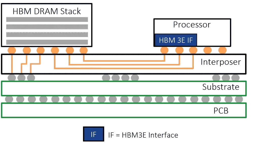
A 2.5D package. An HBM stack and a processor are situated on an interposer in the same package. Source: Rambus
Today, TSMC’s CoWoS technology consists of an 80mm x 80mm substrate. In one configuration, the 3.3 reticle size package can incorporate two GPUs or processors, as well as eight high bandwidth memory (HBM) stacks. Basically, HBM is a stack of DRAM dies.
The company is working on a new version of CoWoS for even larger chips. With a 100mm x 100mm substrate, the 5.5 reticle size package can incorporate two GPUs or processors, and 12 HBM stacks.
Then, the company plans to bring a 9.5 reticle size CoWoS to volume production in 2027, enabling integration of four chips and 12 HBM stacks. The substrate size: 120mm x 150mm.
3-Turblument business climate
The business climate is cloudy, if not turbulent, in the semiconductor industry today.
AI is a hot market in the semiconductor industry. But the non-AI chip markets, such as automotive, consumer and industrial, remain sluggish. Then, there are several other issues in the marketplace, including geopolitical issues, tariffs and trade wars.
Citing the tariffs and other factors, one research firm recently lowered its growth forecast for semiconductors in 2025. “For 2025 IC semiconductor growth, including memory, we now expect unit, ASP, and revenue to be +7% (vs. +11% prior), +5% (vs. +3% prior), and +13% (vs. 14% prior), respectively,” said John Vinh, an analyst with KeyBanc Capital Markets, in a research note.
It’s not all doom and gloom. In fact, there are number of growth drivers for the semiconductor industry. In a presentation, Kevin Zhang, senior vice president of business development and global sales and deputy co-COO of TSMC, listed some of the big growth drivers in the industry, including:
*AI—Demand for AI-related chips, such as AI accelerators, GPUs and HBM, will remain robust in the data center.
*Automotive—Semiconductor content continues to increase in cars.
*Robotics--The next big thing is humanoid robots. These systems will require new processors, microcontrollers, power management ICs and other chips.
*AR/VR--These systems require a 10x improvement in power, cost and form factor, according to Zhang.
Smartphones, PCs, servers and TVs will continue to drive the growth in the semiconductor industry. Other drivers include medical electronics, military/aerospace, quantum computing, among others.
4-Next-gen memories for embedded apps
There is a lot of activity in the embedded memory market. This is especially true in the next-generation memory space, such as MRAM, ReRAM and others.
Embedded memory is a simple concept. The idea is that you embed a tiny memory block in a chip. The microcontroller (MCU) is one example here. An MCU is a chip that is used to power and control a system. MCUs are used in appliances, cars, industrial equipment, medical products and other systems.
Typically, an MCU integrates a CPU, memory and other chip functions in the same device. In an MCU, the memory is called embedded memory. And in many cases, NOR flash memory is the technology of choice for embedded memory. NOR flash memory, a non-volatile technology, is typically used for code storage applications in systems.
Today, the most advanced MCUs are manufactured using a 28nm or 22nm process. These MCUs incorporate embedded NOR flash memory, also based on a 28nm or 22nm process. At the 28nm and 22nm process nodes, though, NOR flash memory is nearing its physical limits.
That’s where emerging memories like MRAM and ReRAM fit in. MRAM and ReRAM are fast and non-volatile with low power and high endurance. They are targeted to replace NOR flash for embedded memory applications at the 28nm/22nm nodes and below.
In 2022, TSMC offered 40nm, 28nm and 22nm embedded ReRAM technologies for foundry customers. Now, the company is releasing a 12nm ReRAM technology. 7nm and 6nm ReRAM technologies are in R&D.
TSMC has also developed a 22nm embedded MRAM technology. It is readying a 16nm embedded MRAM technology. 12nm and 5nm versions are in R&D.
5-HBM4 race
Micron, Samsung and SK Hynix are racing each other to ship next-generation HBM4 products.
SK Hynix appears to be leading the race, at least for now. In March, the company began sampling a 12-layer HBM4 device.
At the TSMC event, SK Hynix was showing an HBM4 product, which is capable of stacking up to 16 DRAM devices. It has a capacity of up to 48GB with an I/O speed of 8Gbps and a bandwidth of 2.0TB/second.
SK Hynix hopes to ship HBM4 by year’s end.