


AI Packaging, CPO, Hybrid Bonding Featured At ECTC
These are important technologies, but why do we need them?

By Mark LaPedus
At the upcoming IEEE Electronic Components and Technology Conference (ECTC), companies, R&D organizations and universities are expected to present papers on the latest breakthroughs in semiconductor packaging and related topics.
ASE, IBM, Intel, Nokia, Nvidia, Samsung, SK Hynix, Sony, TSMC and others will present papers at ECTC. Some of the papers represent technologies that are still in R&D. Others are in production.
The papers will cover a wide range of topics, including co-packaged optics, flexible systems, heterogeneous integration, hybrid bonding and reliability. (Click here to get a sneak peak of some of the papers at the event.)
The event is scheduled from May 27-30 in Dallas, Texas. More than 2,000 scientists, engineers and businesspeople from over 20 countries are expected to attend, along with more than 135 exhibitors.
What is packaging?
Packaging is an important part of the semiconductor industry. In the semiconductor process flow, a company first designs a chip line using specialized software tools. Then, a chipmaker (i.e. Intel, Samsung, TSMC) manufactures the chip line based on that design in a large facility called a fab.
After the chips are fabricated, the devices are sent to a separate facility. Then, the processed chips are assembled into a package. A package is a small enclosure that protects a chip from harsh operating conditions. More importantly, a package helps boost the performance of a chip.
In some cases, a package will consist of a single die or chip. In other cases, a package will consist of two or more dies. For a multi-die product, the goal is to incorporate all dies in the same package. There are several ways to do this, including:
*The dies are placed side-by-side in the same package
*The dies are vertically stacked in the package
*Some dies are placed side-by-side, while others are stacked all in the same package
Each option is viable. The decision to use one option over the others depends on the application.
Flip-chip to hybrid bonding
Stacking chips in a package has several advantages. By stacking, you can integrate more dies in the package. Plus, you can reduce the overall size of the package.
In packaging, there are several ways to stack dies and connect them, including a technology called flip-chip. In flip-chip, tiny copper microbumps are formed on the I/O pads on top of a die. The die is then flipped and placed on a substrate.
The bumps connect the die and the substrate together in a package, according to Integra Technologies. “(Copper bumps) serve as conduits for electrical signals to travel from one part of the chip to another,” according to Techlevated, a technology site.
In another example, tiny copper microbumps are formed on the top of two dies. One die is flipped and connected to the other die. Thus, the dies are vertically stacked and connected.
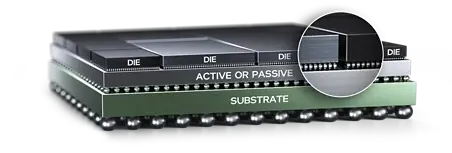
Figure 1. Intel’s Foveros-S 2.5D. A next-generation multi-die package. Bumps connect the dies to the substrate. Source: Intel
In today’s advanced packages, the most advanced microbumps are tiny structures with 40μm to 36μm pitches. A pitch refers to the center-to-center distance between two adjacent bumps.
It’s possible to scale the bumps down to 10μm pitches. But beyond that, the bumps run into mechanical and reliability issues.
So beyond 10μm pitches, the industry needs a new interconnect solution. That’s where hybrid bonding fits in. Hybrid bonding connects chips using tiny, direct copper-to-copper bonds. It enables dense interconnects at 10μm pitches and beyond.
“It enables ultra-fine pitch and small contact sizes, facilitating high I/O counts,” said Yu-Han Chang, an analyst at IDTechEx. “This innovative technique involves embedding metal contacts between dielectric materials and using heat treatment for solid-state diffusion of copper atoms, thereby eliminating the bridging problem associated with soldering.”
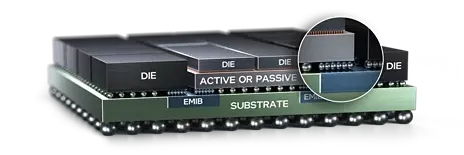
Figure 2. Intel’s Foveros Direct 3D. Stacking and connecting chiplets on an active base die using hybrid bonding. Source: Intel
To enable this process, a company would typically use a hybrid bonding system. Basically, in this system, two separate chips are connected and bonded together using direct copper-to-copper bonds. The system can be used for wafer-to-wafer or die-to-wafer bonding.
Hybrid bonding isn’t new. For some time, this technology has been used in various chip applications, such as 3D NAND, CMOS image sensors and processors. Clearly, hybrid bonding is an enabling technology, but there are some challenges here. Hybrid bonding is expensive. It also involves a complex process.
In response, several entities are working on new approaches for hybrid bonding. At ECTC, for example, National Yang Ming Chiao Tung University and Tokyo Ohka Kogyo will describe a different hybrid bonding approach--copper/polymer hybrid bonding. Researchers demonstrated a 30-second, 150-200° C copper/polymer hybrid bonding process. This low-cost approach has a large process window. It also achieves similar results compared to the traditional oxide-based approaches.
At ECTC, Intel will describe the latest developments in the use of fluidic self-alignment to increase die-to-wafer hybrid bonding throughput. Intel unveiled this process at last year’s ECTC. The fluidic approach is expected to increase the throughput by more than 10x versus current hybrid bonders.
“It makes use of capillary action for fast, precise alignment of a chiplet to a bottom wafer,” according to Intel in an abstract. “First, top dies and bottom wafer are lithographically patterned to create liquid-confinement features around the bonding areas. Then, liquid is dispensed to form a droplet in the center of each bonding area on the bottom wafer. The top dies are transferred onto the droplets, which then spread out to the confines of the patterned area on the bottom surface. Capillary forces from the liquid’s high surface tension align the dies to the lithographic patterns on the bottom wafer. The liquid is subsequently evaporated.”
This year, Intel will describe new details about the technology, including 1) a new process flow with plasma dicing; 2) changes to wafer processing to ensure self-aligned feature compatibility with the hybrid bonded copper pads; 3) assembly process optimization for yield and throughput improvements, and 4) fabrication and initial testing of an electrical test vehicle with hybrid bonded self-alignment features.
Packaging for AI
Besides hybrid bonding, AI is also a hot topic in packaging. Several entities are developing packages for the latest AI chips, particularly for data center applications.
There are several dynamics at play here. In 2024, the world generated 1.5 times the digital data as compared to 2022, according to KKR, a global investment fund.
In many cases, the data is processed and distributed in large facilities called data centers. A large-scale facility, called a hyperscale data center, is a building that contains at least 5,000 servers and occupies 10,000 square feet of physical space, according to IBM.
A server, or a computer, comes in different sizes and configurations. For data-intensive AI workloads, data center operators tend to use AI servers, which are souped-up systems with the latest chips. AMD, Nvidia and others have separately developed various AI chip architectures, which are designed to process the latest AI algorithms in these servers.
Generally, in an AI chip architecture, a company will incorporate a GPU, high bandwidth memory (HBM) and other chips in a 2.5D package. In one 2.5D configuration, a GPU die is placed on an interposer in the package. HBM is placed next to the GPU on the same interposer.
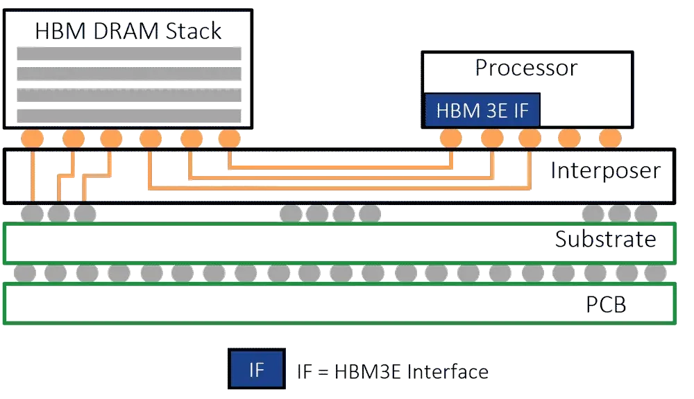
Figure 3. Here’s a 2.5D package. An HBM DRAM stack and a processor or GPU are situated on an interposer in the same package. In operation, the HBM enables the data to transfer between the memory and the processor or GPU at high speeds. Source: Rambus
A GPU is a complex chip based on a parallel processor architecture. HBM is a stack of DRAM dies, which are vertically connected using through-silicon vias (TSVs). HBM enables data to transfer between the GPU and memory at high speeds.
2.5D packages are proven and work in the data center, but there are some challenges here. First, 2.5D packages are expensive. Second, the complexity increases as you add more DRAM dies to the HBM stack. Third, heat becomes an issue here. And finally, TSVs introduce issues such as potential void-free filling, stress management problems and increased fabrication complexity.
At ECTC, Hana Micron, a South Korean OSAT, will present a new type of AI chip architecture—the heterogeneous integrated chip (HIC). HIC uses bridge dies and copper posts instead of a conventional silicon interposer. It also integrates signal and power routing within the bridge die structure and copper posts.
“As a result, routing path lengths are reduced, parasitic RC delays are lowered, and power delivery network formation is simplified, improving both signal and power integrity. The proposed design supports up to 6.4 Gbps per lane in a staggered configuration, suitable for HBM3,” according to researchers.
GPU-based architectures are processing the most advanced AI algorithms in the data center. But to reduce the workloads in the data center, the industry wants to process some AI algorithms on the edge of the network.
Edge computing using AI-enabled image sensors is one possible solution here. For this application, Sony will present a paper at ECTC, which will describe a 1/1.3-inch, 50-megapixel CMOS image sensor. The three-layer image sensor consists of a built-in deep neural network. Potentially, AI-enabled image sensors are capable of processing image data for face and object recognition.
Co-package optics to the rescue
As stated, data centers are large facilities, which consist of a multitude of servers as well as storage devices and other equipment. All of these systems are connected using a complex network.
Up to 76% of all data center traffic traverses inside the data center itself, according to Alphawave Semi. As a result of this traffic, the data center network is prone to bottlenecks and latency. So, data center operators are looking for new and different ways to speed up the network.
Meanwhile, in a typical data center, the servers are incorporated in a rack. Each rack may have eight or more servers. The servers in the rack communicate with each other via copper cabling.
Generally, a system called a switch is situated on top of the server rack. This is sometimes called a top-of-rack (ToR) switch. Basically, a switch is a piece of equipment that transmits data to and from the servers to other equipment in the data center via a high-speed fiber-optic network. The switch itself incorporates several chips, such as an ASIC and other components, on a board.
Meanwhile, at a certain distance from the server rack—perhaps a meter or longer—a data center operator will install another set of switches in the facility. Those switches are called leaf switches. Leaf switches are connected to spine switches in a data center. (See below for one example of a data center architecture)

Figure 4. A 5-stage Clos network topology with clusters in the data center. Large-scale data centers connect hundreds of thousands or even more servers, having millions of users. Source: Noction
The ToR switch and leaf switch need to communicate with each other in the data center. To accomplish this task, the data center operator will use a product called a pluggable optical transceiver. A transceiver is a small module, which consists of a digital signal processor (DSP) and other chips.
In simple terms, you take a pluggable optical transceiver and plug it into a port on the back of the ToR switch. Then, you plug another transceiver into the back of the leaf switch.
A fiber-optic cable connects the pluggable optical transceiver in the ToR switch to the transceiver in the leaf switch, thereby allowing data traffic to flow back and forth from the servers to the ToR switch, and then to the leaf switch. The same interconnection scheme is used to connect the leaf and spine switches.
Pluggable optical transceivers, however, have some limitations in data centers, especially for systems using GPUs in AI applications. “Traditional pluggable optical modules face limitations in signal loss and latency due to long electrical traces,” IDTechEx’s Chang said.
That’s where co-packaged optics (CPO) fits in. In CPO, the optical components are placed next to the ASIC inside the switch equipment. A CPO unit basically replaces a pluggable optical transceiver. “Unlike traditional pluggable modules, CPO integrates optical modules directly onto the switch ASIC substrate, reducing electrical reach and effectively addressing signal integrity issues,” Chang said.
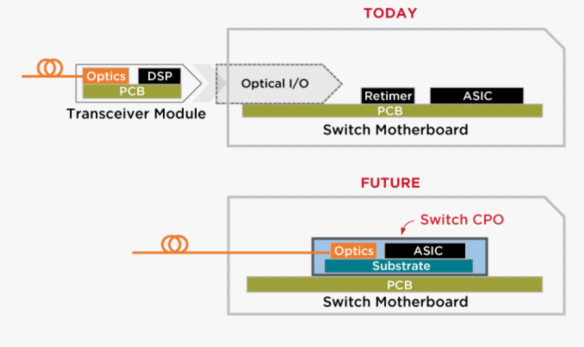
Figure 5. Pluggable transceiver module vs. CPO. By placing the optics next to any ASIC through a single substrate interface, CPO provides the highest level of integration, lowest path loss, and lowest power. Source: Broadcom
In a typical CPO configuration, you might have an ASIC and a silicon photonic integrated circuit. An external laser source is required. The laser supplies the necessary light for signal transmission through the fiber optic network.
The current approach relies on polarization maintaining fiber (PMF) arrays between the external laser sources and the chips to ensure stable polarization states. PMFs provide robust polarization control, but there are some challenges here.
At ECTC, Nvidia will describe an alternative approach that replaces PMFs with single-mode fibers to reduce cost and complexity without compromising system performance.
Also at ECTC, Intel will demonstrate a co-packaged optics assembly technology for fiber-based optical interconnects. Intel will describe the development of a proof-of-concept multi-chip package (MCP) with a novel open cavity bridge substrate. It consists of a compute tile connected through Intel’s Embedded Silicon Bridge (EMIB) technology to two data converter dies on one side, and three photonic IC stacks on the other side with three corresponding fiber array units (56 couplers, 127um pitch) via a fiber-based coupling technology.
CPO using silicon photonics promises to be the next big thing for data centers. For example, Micas Networks, a switch equipment supplier, recently announced the volume production of its 51.2T Co-Packaged Optics (CPO) switch system. Optimized for AI, the CPO switch delivers more than a 40% power consumption savings compared to switches using pluggable transceivers.
Micas’ CPO switch system features Broadcom’s 51.2T Bailly CPO switch device. The device incorporates Broadcom’s Tomahawk 5 switch chip directly coupled to and co-packaged with eight 6.4-Tbps Silicon Photonics Chiplets in Package (SCIP) optical engines.

Figure 6. Broadcom’s 51.2-Tb/s Co-Packaged Optics Switch is a high-radix, high-bandwidth network switching device that supports up to 64 × 800GbE, 128 × 400GbE, 256 × 200GbE, 320 × 100GbE, or 320 × 50GbE ports with integrated optical engines supporting 128xFR4 connectivity. Source: Broadcom
Nonetheless, it’s difficult to describe all of the papers at ECTC. It’s information overload. And the innovations are moving at light speed.