
AMD, Qualcomm Debut New Packaging Technologies
The new memory packaging technologies address the bandwidth bottleneck issues in today’s systems

By Mark LaPedus
Two companies, AMD and Qualcomm, have separately introduced new memory packaging technologies that address the bandwidth bottleneck issues in today’s systems.
In one announcement, AMD has introduced its Versal Premium Gen 2 Memory on Package (MoP) line. Designed for industrial applications, AMD’s new MoP offering incorporates DRAM and a system-on-a-chip (SoC) all in the same package.
Then, in a separate announcement, Qualcomm recently introduced several AI chip products, including a high-end memory packaging technology called High Bandwidth Compute (HBC). HBC is a 2.5D-like memory technology, which addresses the memory bandwidth issues in AI servers.
The respective packaging technologies from AMD and Qualcomm are different and address different market segments. But both packaging technologies have a few things in common. First, they enable faster data transfer rates with reduced latency in systems. Second, both companies claim that their respective technologies have several advantages over existing high-end memory package types, namely high bandwidth memory (HBM).
Based in Santa Clara, Calif., AMD is a supplier of x86-based processors for PCs and servers, as well as FPGAs. Located in San Diego, Calif., Qualcomm is best known as a supplier of chipsets for smartphones.
Qualcomm also sells ARM-based processors for PCs, putting the company in direct competition against AMD and Intel. Now, Qualcomm is moving into the data center with the introduction of a new CPU and AI chip. AMD, Intel and many others also compete in those markets.
What is packaging?
Before describing the new packaging technologies from AMD and Qualcomm in more detail, let’s attempt to answer a simple question: What is packaging?
Packaging is an important part of the semiconductor industry. In the semiconductor process flow, a company first designs a chip line using specialized electronic design automation (EDA) software tools. Then, a chipmaker (i.e. Intel, Samsung, TSMC, others) manufactures a chip line based on that design in a large facility called a fab.
After the chips are fabricated, the devices are sent to a separate facility. Then, in that facility, the processed chips are assembled into an IC package. Basically, a package is a small and rugged enclosure that protects a chip from harsh operating conditions. More importantly, a package helps boost the performance of a chip.
There is no single package that fits every need. In fact, packaging companies offer many package types. Each one is designed for a specific application. Packaging companies provide various packages for automotive, communications, computing and industrial applications.
Another application—AI--is a hot topic today. In AI data centers, computer systems must process complex AI algorithms at high speeds. To process the data, these systems generally incorporate a powerful AI chip, such as an AI accelerator, GPU or related device. Typically, in a system, an AI chip, along with HMB, are incorporated in the same package. This is referred to as a 2.5D package (See Figure 1).
In HBM, you vertically stack 8, 12 or more DRAM dies on top of each other. Then, the DRAM dies are connected using tiny vertical wires called through-silicon vias (TSVs). The TSVs provide the electrical connections between each die.
In operation, HBM enables the data to transfer between the memory and AI chip at high speeds. HBM employs a 1024-bit memory bus, enabling high bandwidth in systems.
Micron, Samsung and Sk Hynix are the main suppliers of HBM products in the market. All told, HBM is the dominate high-end memory technology for high-end applications like AI.
The problem? DRAM, the memory chip product used in HBM, is in tight supply. Plus, DRAM prices have escalated. Thus, HBM remains in tight supply with high prices. And in many cases, the AI chip and HBM are packaged using TSMC’s 2.5D packaging technology. TSMC’s 2.5D technology, called Chip on Wafer on Substrate (CoWoS), is also in tight supply.
In response, suppliers of memory products are expanding their manufacturing capacities to meet demand. In addition, TSMC is also scrambling to add more CoWoS manufacturing capacity.
Still, thanks to AI, DRAMs are expected to be in tight supply through 2027 and perhaps beyond. This presents a major headache for the entire industry.
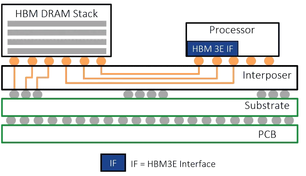
Figure 1. HBM is a DRAM memory stack. HBM is often situated in a 2.5D package. An HBM DRAM stack and a processor or GPU are situated on an interposer in the same package. In operation, HBM enables the data to transfer between the memory and the processor or GPU at high speeds. Source: Rambus
Way of the Dragonfly
The supply chain woes are beyond the control of many. But as before, the semiconductor industry continues to innovate despite the challenges. In fact, some believe that the industry needs new and better packaging solutions.
For example, Qualcomm recently introduced its new Dragonfly chips for AI data centers, including the C1000 CPU, AI300 inference accelerator and a custom silicon offering. The company also rolled out HBC.
In many ways, HBC resembles a 2.5D package with HBM. In HBC, Qualcomm places an AI chip in a 2.5D package. Then, LPDDR DRAM dies are stacked on top of each other, and placed in the same 2.5D package. The AI chip and DRAM stack are side-by-side in the same package, according to a video clip from Qualcomm.
HBC is designed to enable a 6x increase in bandwidth per watt versus HBM, according to Qualcomm. HBC is designed to enable a 200x increase in capacity per watt versus SRAM, according to the company.
Initially, Qualcomm will incorporate HBC within its AI250 data center rack, which is a rack-scale AI inference platform. “Qualcomm says HBC combines accelerator logic with 3D-stacked DRAM in a tightly coupled package,” said Jon Peddie, president of Jon Peddie Research, a research firm, in a blog.
“Qualcomm describes HBC as a memory-centric accelerator architecture. The design keeps data closer to compute, reduces movement across external interfaces, and improves bandwidth efficiency,” Peddie said.
It’s a promising solution. “Qualcomm’s HBC approach puts memory bandwidth, packaging, and power at the center of system design. The inflection point emerges as hyperscalers and enterprises evaluate AI racks through total cost, software portability, and supply resilience. If Qualcomm delivers, AI data centers could support more diverse architectures and reduce dependence on a single software-hardware model,” Peddie said.
Still, there are some unanswered questions about HBC. “Silicon teams will want details on packaging, thermals, yield, repair, memory supplier support, interconnect topology, and compiler visibility. CIOs will focus on rack power, cooling, utilization, procurement timing, cloud access, service support, and software compatibility,” Peddie said.
Commercial sampling of HBC Gen 1 with AI250 is expected in mid-2027.
More advanced packaging
To be sure, AI in the data center tends to grab the headlines these days. But as before, there is a huge semiconductor market beyond data centers. These chip markets, such as automotive, communications, industrial and others, are also important.
Looking to address some of these markets, AMD has introduced the Versal Premium Gen 2 MoP technology. Basically, AMD’s MoP offering combines its Versal chip line and DRAM in the same package. AMD’s Versal is a general-purpose system-on-a-chip (SoC) product line.
In total, AMD’s MoP technology can integrate up to 32GB of LPDDR5X DRAM into a single SoC package, delivering up to 288GB/s of bandwidth in up to 60% less board area.
“AMD places standard JEDEC-compatible LPDDR5X devices on the package substrate alongside the Versal compute die,” Peddie explained in a separate blog. “The short interconnect distances eliminate external memory routing, simplify board design, reduce validation effort, and improve signal integrity. AMD estimates more than 60% board-area savings compared with an equivalent discrete-memory implementation. The company also claims that designers can eliminate months of memory-interface design, simulation, qualification, and board-level validation work.”
AMD’s MoP technology is targeted for embedded and industrial applications. As physical AI, networking, aerospace and defense workloads push more data through ever-tighter space and power budgets, MoP targets the designs that need it most: test and measurement, professional video editing, and VPX systems for secure communications and defense acceleration. VPX refers to a rugged, high-performance embedded computing standard (VITA 46) used in aerospace, defense and industrial applications.
Built for long life cycles and industrial-grade environments, AMD’s MoP solution offers 15-plus-year support to help reduce design risk and protect product roadmaps from HBM’s shorter, data-center-driven refresh cycles.
“The target applications reveal where AMD sees demand emerging. Physical AI systems require local processing of sensor data with minimal latency. Networking platforms need larger packet buffers and faster data movement. Radar and electronic-warfare systems process large datasets in real time. Professional video systems require substantial image buffering and AI-assisted enhancement. Test-and-measurement equipment captures and analyzes increasingly large data streams. Each workload places pressure on memory bandwidth and memory capacity while operating within constrained physical footprints,” Peddie said.
AMD Versal Premium Gen 2 MoP devices will begin sampling at the end of 2026 with production shipments expected to begin in the second half of next year.
Still more packaging
Others have also recently introduced new high-end memory packaging technologies, including High Bandwidth Flash (HBF) and Z-Angle Memory (ZAM).
SK hynix and Sandisk are pushing HBF. Both companies have started the standardization process for HBF.
Meanwhile, SoftBank’s subsidiary, SAIMEMORY, recently signed a collaborative agreement with Intel. The companies plan to commercialize ZAM, a next-generation memory technology designed for high capacity, high bandwidth and low power consumption.