CEA-Leti, Imec launch chip pilot lines
Europe’s CHIPS Act fuels new and ambitious semiconductor projects, such as two chip pilot lines, in the EU.
By Mark LaPedus
The European Union (EU) is taking steps to bolster its semiconductor industry.
Two European R&D organizations, CEA-Leti and Imec, are separately spearheading a pair of new semiconductor pilot lines in Europe. The Imec-led pilot line involves sub-2nm logic chip technologies. Both pilot lines enable European and international companies to conduct R&D and explore new technologies before they are introduced into mass production. Other chip programs are also in the works in the EU.
These initiatives are part of a new and ambitious program called the European Chips Act. Announced in 2022, the European Chips Act involves a $47 billion program to strengthen the EU’s semiconductor ecosystem. As part of the plan, the EU also hopes to boost Europe’s share of semiconductors from 8% in 2021 to 20% by 2030.
The United States and other nations have launched similar national chip programs—and for good reason. Semiconductors, or chips, are small and critical devices used to power a multitude of products, such as appliances, cars, industrial equipment, medical products, PCs and smartphones.
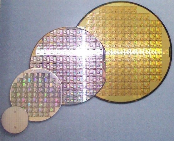
Source: Wikipedia
Basically, companies use specialized software tools to design a chip. Then, chips are put into production in large, expensive fabs. Each advanced fab can cost from $10 billion to $20 billion today.
However, China, Korea and Taiwan produce a large percentage of today’s chips. But this region is a geopolitical hotspot. Any disruption in this region could potentially impact the supply of chips.
The recent Covid pandemic was especially disruptive. During that period, there were bottlenecks in the worldwide supply chain, causing acute shortages of chips.
With the European Chips Act, the EU hopes to address these and other issues. For decades, Europe has been an important part of the worldwide semiconductor industry. The EU is the home to many semiconductor companies, including Infineon, NXP, STMicroelectronics and others.
But over the years, the EU’s share of the worldwide semiconductor market has dwindled. The same is true with the EU’s overall semiconductor production capacity. Plus, there are no leading-edge production fabs in the EU.
In response, the EU in 2021 outlined a new vision for Europe’s chip strategy, hoping to create a state-of-the-art semiconductor ecosystem. This involves new R&D initiatives and chip production. The EU also hopes to connect its research, design and testing capacities.
New chip pilot lines
This, in turn, evolved into the European CHIPS Act. As part of those efforts, CEA-Leti and others this week launched the FAMES Pilot Line, a project aimed at advancing semiconductor technologies in Europe.
France-based CEA-Leti is the pilot line coordinator. Other members of the FAMES group include Imec, Fraunhofer Mikroelektronik, Tyndall, VTT, CEZAMAT WUT, UCLouvain, Silicon Austria Labs, SiNANO Institute, Grenoble INP-UGA and the University of Granada.
With a total of US$889 million in funding, the pilot line will develop five new sets of technologies:
*FD-SOI. The goal is to develop two new FD-SOI technology nodes at 10nm and 7nm.
*Next-generation memories. The plan is to propel the development of several types of embedded non-volatile memories, such as OxRAM, FeRAM, MRAM and FeFETs.
*RF components. The plan to develop next-generation switches, filters and capacitors.
*Two 3D integration options. The idea is to further develop two manufacturing technologies--heterogeneous integration and sequential integration.
*Small inductors. The goal is to develop DC-DC converters for power management integrated circuits (PMICs).
Meanwhile, in a separate announcement, Belgium-based Imec recently announced that it will spearhead and host the NanoIC pilot line.
Besides Imec, this group includes CEA-Leti, Fraunhofer, VTT, CSSNT and Tyndall National Institute.
With a total investment of US$2.68 billion, the NanoIC pilot line group will focus on three research pillars:
*Advanced logic. The group will develop the processes and modules to enable the integration of gate-all-around nanosheet transistors beyond the 2nm technology node. The group will also develop a complementary field-effect transistor (CFET) baseline flow targeting the A7 logic technology node.
*Advanced memory technology. The group will further develop spin-orbit torque magneto-resistive random-access memory (SOT-MRAM) architectures, embedded DRAM (eDRAM) technology and a 3D memory platform.
*Advanced interconnect technologies. The group plans to advance the development of 3D electrical interconnects for scaled-pitch die-to-wafer hybrid bonding and high-density redistribution layer (RDL) technologies optical interconnects, such as active silicon photonics interposers and GaAs quantum dot chiplets for hybrid bonding.
“The investment will allow us to double volumes and learning speed, accelerating our innovation pace, strengthening the European chip ecosystem, and driving economic growth in Europe,” said Luc Van den hove, president and chief executive of Imec.


