


Europe Opens Advanced Packaging Pilot Line
The project, funded by the European Chips Act, will focus on chiplets and other technologies.

By Mark LaPedus
With funding from the European Chips Act, a consortium led by Fraunhofer has opened an advanced packaging pilot line in Berlin, Germany.
The pilot line consortium, called APECS (Advanced Packaging and Integration for Electronic Components and Systems), plans to develop new breakthroughs in advanced packaging. The overall funding for APECS is €730 million (US$760.4 million) over 4.5 years.
The APECS pilot line consortium is coordinated by Fraunhofer-Gesellschaft, a German R&D organization. APECS resides at the Research Fab Microelectronics Germany (FMD) organization. FMD is a cross-location research cooperation between Fraunhofer and the Leibniz Institute.
In addition to Fraunhofer and Leibniz, the other members of the APECS consortium include CEA-Leti (France), Imec (Belgium), VTT (Finland), TU Graz (Austria), FORTH (Greece), IMB-CNM, CSIC (Spain) and INL (Portugal).
APECS will focus on application-oriented research in advanced packaging, heterogeneous integration and chiplets. The goal is to boost Europe’s capabilities in these areas.
What is packaging?
Packaging is an important part of the semiconductor industry. In the semiconductor process flow, a company designs a chip line using specialized software. Then, a chipmaker manufactures the chip line based on that design. Finally, the chip line is assembled in a package.
A package is a product that forms a protective case or enclosure for a given chip line. The package protects the chip from harsh operating conditions. Over the years, the semiconductor industry has developed a multitude of different package types. Each type is geared for a specific application.
Some packages are simple, commodity-level products, which are used for more mature chip types. Some are considered mid-range packages, which are used for more advanced chips. Still others are classified as advanced packages, which are used for the most complex chips, such as FPGAs, GPUs and processors.
An advanced package is used to boost the overall performance of a given chip line. Generally, advanced packages incorporate multiple and different chips in the same unit. Incorporating different dies in a package is sometimes called heterogeneous integration.
There are several types of advanced packages in the market. The chiplets concept, one form of advanced packaging, is gaining steam. In chiplets, the idea is to take a large device like a processor. Then, you break up that device into smaller dies. Then, the dies, or chiplets, are assembled in an advanced package. The idea behind chiplets is to reduce the cost of an advanced chip design.
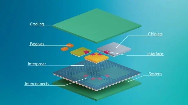
Chiplets allow the integration of various and different functional dies on a substrate or into a 3D chip structure. Source: Fraunhofer IIS/EAS
EU CHIPS Act
A number of governments, companies, R&D organizations and universities are working on advanced packaging and chiplets. For example, several entities within the European Union (EU) have been working on these and other technologies. APECS is the latest effort in the EU.
“Together with the other EU Chips Act pilot lines, APECS will be a crucial component for heterogeneous integration and advanced packaging of the envisioned pan-European pilot line facility – and thus an indispensable instrument of the EU Chips Act,” said Albert Heuberger, chairman of the FMD.
APECS is one of five pilot lines in the EU that have been established and funded under the European Chips Act. Announced in 2022, the European Chips Act involves a $47 billion program to bolster the EU’s semiconductor ecosystem. As part of the plan, the EU hopes to boost Europe’s share of semiconductors from 8% in 2021 to 20% by 2030.
Besides APECS, the other pilot lines in the EU include:
*FAMES--FD-SOI pilot line as well as R&D for non-volatile embedded memories, RF and 3D integration. Coordinator: Leti in France.
*NanoIC—Pilot line for technologies beyond 2nm. Coordinator: Imec in Belgium.
*PIXEurope--Advanced photonic integrated circuit pilot line. Coordinator: ICFO in Spain.
*WBG-- Wideband gap materials pilot line (GaN and SiC). Coordinator: National Council of Research in Italy.
Other nations have also launched their own versions of the CHIPS Act. The United States has a major effort here. China, India, Japan, South Korea and Taiwan have separately launched various programs, which are aimed to boost their domestic semiconductor industries.
More packaging
Meanwhile, besides APECS, there are other major developments on the packaging front in Europe. For example, Singapore’s Silicon Box, a panel-level packaging and chiplet foundry, recently announced plans to establish a $3.6 billion facility in Italy. The EU has approved partial funding for the facility.
In a separate development, the Fraunhofer Institute for Reliability and Microintegration IZM recently launched a Glass Panel Technology Group. This initiative aims to develop glass-based substrates for advanced packaging. In addition, the organization also recently launched an automotive chiplet R&D center. These efforts are separate from APECS.
Meanwhile, Imec continues to expand its efforts in the field of chiplets. The Belgium R&D organization recently launched an automotive chiplet program. Then, at the recent 2024 IEEE International Electron Devices Meeting (IEDM), Imec presented a paper on the development of chiplets in the high-end radio frequency (RF) market.
In the IEDM paper, Imec developed dies, or chiplets, using a III-V compound semiconductor material called indium phosphide (InP). Then, Imec devised a way to assemble InP-based chiplets on a 300mm RF silicon interposer.
With the technology, Imec demonstrated a two-stage InP power amplifier device. Still in R&D, Imec’s InP chiplet technology could one day pave the way towards wireless systems in the high-end millimeter-wave (mmWave) frequency range. That involves frequencies above 100GHz.
“By using InP only where its unmatched performance is essential, Imec is paving the way toward scalable, cost-effective mmWave and sub-THz solutions. This is where a chiplet approach becomes essential,” said Siddhartha Sinha, principal member of technical staff at Imec.
“In addition to developing a demonstrator for mmWave phased arrays and radar applications, we aim to further shrink the size of the InP chiplets while preserving their superior RF performance. We also plan to add new Si RF interposer features to the platform, including passives like inductors and MIMCAPs, as well as TSV integration and wafer thinning,” Sinha said. “At the same time, we’re making the platform available to partners for prototyping, allowing them to experiment with Imec’s RF interposer R&D platform.”
(Send comments to: mdlapedus@gmail.com Semiecosystem reserves the right to post and edit comments.)