
IBM Debuts Nanostack Technology For Sub-1nm Chips
Big Blue has unveiled a sub-1nm chip technology, featuring a new transistor architecture at the 0.7nm node

By Mark LaPedus
IBM has unveiled a sub-1nm chip technology, featuring a new transistor architecture at the 0.7nm or 7 angstrom node.
IBM’s chip technology is based on the company’s new “nanostack” transistor architecture. Nanostack is a 3D-like technology, which represents a new and different way to scale semiconductor devices in the future.
But don’t expect nanostack-based chips anytime soon. With the expectation of the earliest adoption of nanostack technology at the sub-1nm node, IBM sees a path to production in as early as the next five years.
Basically, a transistor is a key building block in a chip. Transistors are tiny structures used to amplify or switch electrical signals in the device. Today’s advanced chips integrate billions of tiny transistors in the same device.
Nonetheless, IBM’s nanostack technology makes use of 3D nanosheet-based design techniques. “The nanostack design vertically stacks and staggers transistors, taking advantage of 3D sequential integration to pack more transistors onto a chip. The design also unlocks the use of different material combinations within each stacked layer, optimizing performance and power efficiency of each transistor independent of the other,” according to IBM.
IBM’s new sub-1nm chip packs nearly 100 billion transistors onto a chip the size of a fingernail, nearly twice the density of IBM’s 2nm chip unveiled in 2021, according to Big Blue.
At the recent VLSI Symposium, IBM demonstrated that the nanostack architecture provides a 40% scaling benefit for SRAMs. In general, a 0.7nm nanostack chip provides up to 50% more performance, or 70% greater energy efficiency, than IBM’s 2nm node chips.
Potential applications for nanostack-based chips range from generative AI and cloud infrastructure to next-generation electronic devices. “IBM’s latest chip breakthrough marks a landmark moment in computing, pushing technology beyond the nanometer era to the scale of atoms. With our new nanostack architecture, we’re not just making smaller transistors, we’re reinventing how chips are built to deliver dramatically more power and energy efficiency,” said Jay Gambetta, director of IBM Research and IBM Fellow.
Nanostack vs CFETs
Still, the question is clear: When will IBM’s nanostack technology appear in the market? To be sure, it won’t appear in the near term. It may never appear.
Today, leading-edge chipmakers, namely Intel, Samsung and TSMC, are manufacturing chips based on their new and respective 2nm process technologies. Today, 2nm represents the world’s most advanced process.
The new 2nm chips are based on a newfangled transistor architecture called gate-all-around (GAA). More specifically, chipmakers are ramping up a GAA technology called a nanosheet field-effect transistor (FET). Nanosheet technology was invented by IBM.
The nanosheet FET is expected to extend for at least three process generations, including the 2nm, A14 and A10 nodes. Then, at some point in the future, nanosheet FETs could run out of steam.
After the nanosheet FET, the complementary field-effect transistor (CFET) is the next leading logic transistor candidate on the roadmap (See Figure 1). In R&D, Intel, Samsung, TSMC and others are developing CFETs. Based on the roadmap, CFETs could appear at the A7 technology node in 2031.
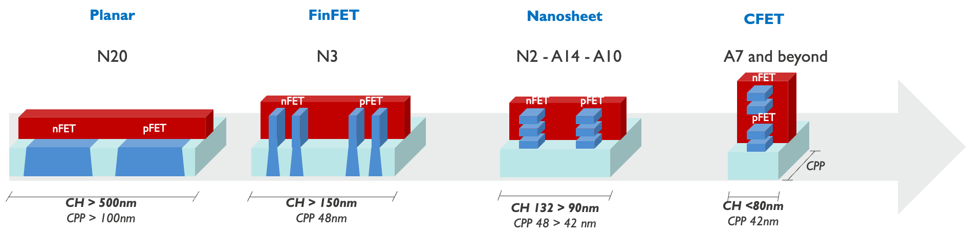
Figure 1. The evolution of the transistor. Planar and finFET transistors are in production today. Nanosheets FETs are ramping up. CFETs are on the horizon. Source: Imec
What about nanostack?
Meanwhile, for the same timeframe, IBM is developing another possible future transistor option for chips--nanostack technology. As stated, IBM sees a path towards production as early as the next five years.
In other words, CFETs and nanostack transistors could be viewed as competitive technologies. CFETs are different than nanostack technology. In CFETs, the NFET and PFET transistors are stacked on top of each other in a vertical fashion.
Nonetheless, the semiconductor industry doesn’t have the resources to develop both the CFET and nanostack technologies. Simply put, it’s too expensive.
So, the industry will eventually rally around one technology. Right now, CFETs have the most momentum, but the industry is always searching for a better solution.
If CFETs and nanostacks fail to make it into production in the future, the industry still has several backup options. Advanced packaging and chiplets may prevail in the long term.
Today, for leading-edge devices, chip vendors tend to integrate all functions on a large monolithic die. That’s becoming too expensive for some chip designs. In chiplets, the idea is to develop smaller dies with different functions. Then, the dies assembled into an advanced package. That’s fast becoming the main option for today’s advanced AI chip designs.
Appreciate for wonderful information