Imec, TSMC, Samsung-IBM Make Progress With CFETs
Still in R&D, CFETs are 3D-like transistors that may appear in the 2030s.
By Mark LaPedus
At this week’s 2024 IEEE International Electron Devices Meeting (IEDM) in San Francisco, Imec, TSMC, the Samsung-IBM duo and others will present papers on a next-generation technology called the complementary field-effect transistor (CFET).
Still in R&D, the CFET is a 3D-like transistor structure that represents a major leap from today’s technologies. CFETs may appear in chips sometime in 2031 or beyond, but there are still a multitude of technical and cost challenges in order to develop and produce them. CFETs may never appear, if the industry is unable to overcome these challenges. If CFETs fail to make it into production in the future, the industry still has several backup options.
A transistor, which is a key building block in a chip, is a tiny structure used to amplify or switch electrical signals in the device. Transistors come in two flavors: n-channel transistors (NFETs) and p-channel transistors (PFETs). An advanced chip consists of billions of tiny transistors in the same device.
For over a decade, chipmakers have been manufacturing the most advanced chips using a transistor type called the finFET. Soon, finFETs will run out of steam. So today, the industry is preparing to make the transition to a new transistor type called gate-all-around (GAA). Some call it the nanosheet FET.
Then, at some point in the future, GAA could hit the wall. After GAA, the CFET is the next leading logic transistor candidate on the roadmap. Based on Imec’s roadmap, CFETs could appear at the A7 technology node in 2031.
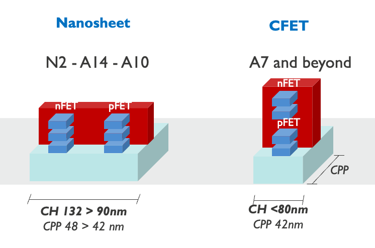
CFETs are different than today’s transistors. In finFETs and GAA, the NFET- and PFET-type transistors are situated next to each other on a substrate. In CFETs, the NFET and PFET transistors are stacked on top of each other in a vertical or 3D fashion, which in turn provides several benefits. “In CFETs, you save on area by moving the NFET on top of the PFET or vice versa,” said Geert Hellings, program director at Imec.
In R&D, Imec, Intel, Samsung, TSMC and others for some time have been separately working on CFETs. Over time, the industry has made incremental progress with CFETs, but there are still a multitude of challenges to develop them. At IEDM, several entities will present papers on their latest research efforts with CFETs, including:
*Imec will describe a double-row standard cell architecture for CFETs, which is targeted for the A7 node. This architecture promises to simplify the CFET process and reduce the cell area.
*TSMC will describe a CFET with a 48nm gate pitch.
*The Samsung-IBM duo will describe a monolithic stacked FET architecture.
The evolution of the transistor. Planar and finFET transistors are in production today with nanosheets in the works. CFETs are on the horizon. Source: Imec
Planar to GAA
An advanced chip consists of a multitude of tiny transistors. Besides making the transistors, a chipmaker will create a tiny wiring scheme on top of these transistors, which connects these structures within the chip. This wiring scheme consists of a complex network of tiny copper interconnects. Some chips have 15 to 20 levels of copper interconnects.
In the manufacturing process, the goal among chipmakers is to shrink, or scale, select features of a tiny transistor by 0.7x every 24 to 36 months, thereby making these structures smaller and faster at each turn. This in turn enables new and faster chips, paving the way towards the next wave of PCs, smartphones and other products.
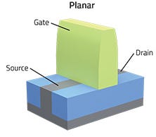
Up until the 2010s, Intel, Samsung, TSMC and others manufactured various types of high-performance chips using tiny planar transistors. In a transistor, the “current conduction between the drain and source is controlled by a voltage applied to the gate terminal,” according to Toshiba.
Planar transistor (Source: Lam Research)
In the 2010s, the planar transistor reached its physical limits at the so-called 20nm process node. A 20nm process consists of a 90nm contacted gate pitch (CPP), according to WikiChip, a technology site. CPP is the horizontal distance between the centers of two adjacent gate contacts.
Planar transistors are still used for chips at the 20nm node and above (i.e. 28nm, 40nm, 65nm, etc.). But at that time, the industry required a new transistor type for high-performance chips beyond 20nm. In 2011, Intel migrated to a new and faster transistor type called the finFET at the 22nm node. Later, GlobalFoundries, Intel, Samsung, and TSMC migrated to finFETs at the 16nm/14nm nodes.
Thanks to finFETs, the semiconductor industry has developed and shipped new and faster chips for several generations. Today, TSMC has extended the finFET to the 3nm node. At 3nm, TSMC is making leading-edge chips for Apple and others. Generally, the 3nm node consists of a 48nm CPP with a 150nm or larger cell height, according to Imec.
Planar vs finFET transistor (Source: Lam Research)
FinFETs, however, will run out of steam beyond the 3nm node. So starting at the 2nm node in 2025, TSMC is expected to ramp up chips based on a new transistor type called GAA. Some call it the nanosheet FET.
In 2022, Samsung began shipping chips based on nanosheets at the 3nm node. But Samsung is struggling with its yields here. To be sure, nanosheets provide better performance than finFETs, but they are harder and more expensive to make in the fab.
There are other challenges. On the transistor, the copper interconnects are becoming too congested, potentially causing a power drop in the device. So at some point, Intel, Samsung and TSMC will combine the nanosheet FET with a new technology called a backside power delivery network (BSPDN).
“With backside power delivery, the entire power distribution network is moved to the wafer’s backside,” said Julien Ryckaert, vice president of logic technologies at Imec, in a blog. “Because backside power-delivering interconnects can be made larger and less resistant, BSPDN is believed to reduce on-chip IR drop significantly.”
Nonetheless, the nanosheet FET is expected to extend for at least three process generations, including the 2nm, A14, and A10 nodes. At these nodes, the CPPs for nanosheet FETs are 48nm to 42nm with cell heights from 132nm to 90nm.
Planar vs finFET vs GAA transistor (Source: Lam Research)
CFET challenges
At some point in the distant future, the nanosheet FET could run out of steam. The CFET is the next transistor type on the roadmap. Targeted for the A7 node in 2031, the CFET may consist of a 42nm CPP with cell heights below 80nm, according to Imec.
The CFET is a 3D-like transistor with a BSPDN structure. There are two ways to make CFETs—the monolithic or sequential approach. In the monolithic approach, the NFETs and PFETs are manufactured in a continuous fashion in a fab. In sequential, the bottom device is developed on one wafer. The top device is made on a second wafer. The two wafers are bonded.
Both approaches are challenging. “The monolithic approach offers better performance and lower cost. However, extremely high aspect ratio (HAR) etching is needed for monolithic integration,” according to a technologist from Lam Research in a blog. “The sequential approach allows more flexibility in NFET and PFET channel materials. However, a very accurate NFET-PFET alignment is needed using sequential integration. Additionally, thermal budget is also a concern.”
The monolithic approach is gaining steam, but there are other challenges. At the circuit level, there are several options for integrating the CFET into a standard cell architecture. One challenge is the middle-of-line (MOL) connectivity in the BSPDN. This involves interconnects that connect source/drain and gate contacts to the first metal lines and ensure top-to-bottom connectivity for both power and signal, according to Imec. A complex and area-inefficient MOL could negate any benefits for CFETs.
The optimal option, according to Imec, is a double-row CFET architecture. This option simplifies the process, while also offering other benefits. “Our DTCO study shows that one shared MRW (middle routing wall) for every 3.7 FET is sufficient to build logic and SRAM cells,” Imec’s Hellings said. “This allows us to further reduce standard cell heights from 4 to 3.5T, compared to ‘classical’ single-row CFETs. This translates into a significant area reduction of 15% for SRAM cells. Compared to SRAMs built with, e.g., A14 NSH technology, double-row CFET-based SRAMs enable more than 40% area shrinkage, providing a further scaling path for SRAMs.”
Nanosheet (GAA) vs CFET (Source: Imec)
Others are also working on CFETs. At IEDM, TSMC will describe a CFET inverter with a 48nm gate pitch using a monolithic approach. “The devices exhibited well-balanced voltage transfer characteristics up to 1.2V, and a good sub-threshold slope of 74-76mV/V for both n and p devices,” said Sandy Liao, director of R&D pathfinding at TSMC, in a paper. Others contributed to the work.
At IEDM, the team of Samsung and IBM will present a paper on a monolithic stacked FET architecture featuring a stepped channel. This looks like a CFET except the bottom transistor is wider than the top one. “Such a design relieves high aspect ratio process challenges by reducing the total stack height and provides better performance as compared to its uniform channel width counterpart at the same footprint,” said Chen Zhang of IBM, in a paper at IEDM. Others contributed to the work.
Last year, meanwhile, Intel demonstrated a CFET at a scaled gate pitch down to 60nm. Intel also combined the CFET with backside power and direct backside contacts.
Conclusion
All told, CFETs are making progress, but they won’t be ready for some time. But what if CFETs fail to make it into production in the 2030s? At that point, the semiconductor industry still has several other options, including:
1) Extend the nanosheet FET
2) Chiplets
3) 2D FETs using transition-metal dichalcogenide materials
4) Quantum computing devices and systems
All of these options are viable, especially chiplets. Today, the industry is already embracing the chiplet concept. In chiplets, the idea is to break up a large device into smaller dies. Once the dies are fabricated, they are assembled in an advanced package.
Another option may even emerge. The industry has always been innovative and found a way to develop the next wave of systems.
(Send comments to: mdlapedus@gmail.com Semiecosystem reserves the right to post and edit comments.)


