
Inside Packaging And Module Technology With Saras Micro
Company executives discuss the semiconductor industry, advanced packaging and the challenges facing the IC industry in the AI era.

By Mark LaPedus
Ron Huemoeller, chief executive of Saras Micro Devices, and Eelco Bergman, chief business officer of Saras Micro Devices, sat down with Semiecosystem to discuss the semiconductor industry, advanced packaging and the challenges facing the IC industry in the AI era. Company executives also talked about Saras Micro’s new multi-domain embedded module technology for the IC packaging industry.
Semiecosystem: Where are we in the semiconductor cycle? Are we still in a downturn or a recovery mode in the semiconductor industry? And what are some of the key growth drivers here?
Huemoeller: I believe the industry is in the early stages of the next major growth cycle, fueled by the rapid rise in the availability and adoption of AI tools and applications. For the last two decades, the semiconductor cycle has been driven by mobile computing, including handsets, tablets and notebooks, as well as IoT devices, both in consumer and industrial applications. Neither of these markets are going away, but their growth rates have certainly slowed as their penetration saturates. Indications are clear that the next wave of growth has already begun and, for the next five to ten years, it will be driven by AI hardware.
Bergman: I agree with Ron. Over the last two to three years, we’ve started to see a significant increase in the demand for advanced processors, accelerators, and network devices as a result of the extreme compute performance required to support the processing and training of the exponentially growing data sets and model sizes. Today, that demand is driven primarily by the data centers belonging to the CSPs (cloud service providers), and ISPs (Internet service providers), but there will be additional waves of adoption coming from enterprises, autonomous vehicles, industrial, AR/VR, and consumer applications, particularly as the need for inferencing devices near or at the edge start to rise.
Semiecosystem: The large foundry vendors continue to announce new processes at advanced nodes. Yet, we hear that Moore’s Law is slowing down. In other words, traditional chip scaling is supposedly slowing and becoming more difficult at each node. What’s happening with traditional chip scaling?
Huemoeller: The continued advancement of Moore’s Law is becoming more challenging, both from a technical and economic perspective. That much is clear. However, despite the challenges, the leading foundries are all showing roadmaps and progress towards more advanced sub-nanometer processes as well as sustained improvements in PPA (power, performance and area). It’s important to note that the facility construction, tool, material, and process development expenses associated with these leading-edge capabilities are resulting in device design and manufacturing costs that may not be commercially viable for even the most advanced and performance driven products. In addition, for many of these leading devices, the physical size and reticle limitations are slowing the continued SoC (system-on-a-chip) device integration necessary to achieve the functional density and bandwidth required.
Bergman: To compensate for this, the leading device suppliers and manufacturers in the industry are all increasingly adopting chiplet-based architectures and heterogeneously integrated packaging approaches to enable continued PPA scaling at the product level, while optimizing cost performance at the individual chiplet and integrated device level.
Semiecosystem: We are hearing more and more about chiplets. What are chiplets and what are the benefits?
Huemoeller: Although there may not be complete agreement on the definition of a chiplet across the industry, I think everyone is aligned that a chiplet is a device that’s been designed to function in conjunction with other dies or chiplets, not just as a standalone device. Chiplets can result from the heterogeneous or homogeneous partitioning of a larger SoC design or from the independent development of an IP die, such as a SerDes or memory I/O device. In order to function, chiplets need to be co-integrated with other devices utilizing advanced packaging techniques, including silicon/fan-out RDL (redistribution layer) interposers, hybrid bonding and others.
Bergman: The potential benefits of chiplet-based architectures have been well covered, but include the ability to use different, cost/performance optimized foundry nodes for each chiplet that will be used to enable the integrated silicon system. Chiplet-based architectures also reduce design/development costs and cycle times, as well as enable IP chiplet portability/re-use for future designs. Of course, there are also challenges that need to be overcome for mass adoption, starting with the need for some level of standardized interfaces.
Semiecosystem: Years ago, IC packages were relatively simple units that basically encapsulated the chips. In recent times, IC packaging, particularly advanced packaging, has become more important. Why? And what role does packaging play now?
Huemoeller: IC packaging’s role has really evolved and matured from its previous traditional role in the industry to where it is now, that is, providing the enabling technologies and solutions required to fully support the integration of a complete silicon-based system into a single package or module. These advanced packaging capabilities are particularly important for the high-performance compute devices that serve as the processor engines for generative AI systems. In order to support these exponentially growing models, the required advances in processor performance have outstripped the ability of discretely packaged devices to maintain pace. Packaging has answered the call however, by heterogeneously integrating multiple high-performance SoCs, high bandwidth memories and I/O chiplets into singular tightly integrated silicon systems, and enabling the requisite performance, bandwidth, power efficiencies and latencies. The advanced packaging technologies needed to support this are rapidly progressing, particularly those like hybrid bonding to enable increasingly finer pitch (sub-10µm) die-to-die interconnect and fan-out RDL to support 4-6x reticle-sized multi-dimensional device integrations.
Semiecosystem: AI is a hot topic. The latest AI chips, particularly the GPU-based architectures, provide the compute power to drive some amazing capabilities in the AI field. Yet, there are some issues and challenges with these devices in terms of power density and others, right?
Bergman: Yes. AI, particularly the processor and accelerators running the large generative AI models, have really provided the catalyst for the next wave of semiconductor industry growth. Today, these devices, really integrated silicon systems, are primarily running in large data centers and are being pushed to their performance limits. The key metrics that are focused on to enable the ever-increasing device performance required include the core processor performance (TOPS), chip-to-chip bandwidth, memory bandwidth, memory capacity, and power efficiency. As you mentioned, the power density and thermal management challenges resulting from the power delivery needs for these large integrated devices are significant. As the number of dies/chiplets in a package increases, so do the number of power rails and domains that need to be serviced. The most advanced AI devices are operating at 500-1000W or more, and at voltages well below 1V. This results in very high currents, which when routed in from external power conversion devices, incur significant IR routing losses. Since the overall power appetite of the AI data centers/fabs is a major concern, minimizing these inefficiencies in power delivery is critical.
Semiecosystem: What are some of the board-level challenges with these new AI chips and architectures?
Huemoeller: Historically, system boards in server applications were designed with 12V inputs. In many cases, this has transitioned to 48V, which enables lower current, and thus reduced IR losses as the power requirement of these systems increase. However, on the system board itself, this voltage still needs to be stepped down several times to support the increasing number of power rails and domains necessary to drive the increasingly more integrated multi-die processor devices. As a result, the power delivery challenges are becoming increasingly complex as the designers strive to optimize power delivery performance and efficiency across the increasing number of power conversion devices required.
Semiecosystem: I believe Saras is addressing some of these issues, right? What is Saras Tile, or STile, and what are the benefits? Isn’t it like an embedded passive component technology?
Huemoeller: Yes. Saras is focused on providing solutions that will help improve power delivery performance, especially for AI devices. Now that most of the silicon required to drive these advance systems has been integrated into a single package, the next logical step is for designers to start looking at moving some portion of the power management and conversion closer to, or within the package itself. Our initial product is a multi-terminal, multi-domain capacitor module, that we call a Saras Tile or STile. The STile is specifically designed to be embedded directly into the substrate core, within the die shadow, just prior to the addition of the build-up RDL layers. By doing this, we are enabling designers to start a transition from lateral power delivery solutions that encompass higher IR losses, to a vertical power delivery system with much higher efficiencies.
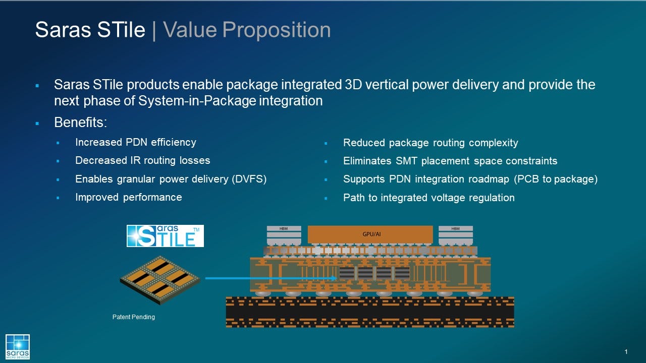
Source: Company
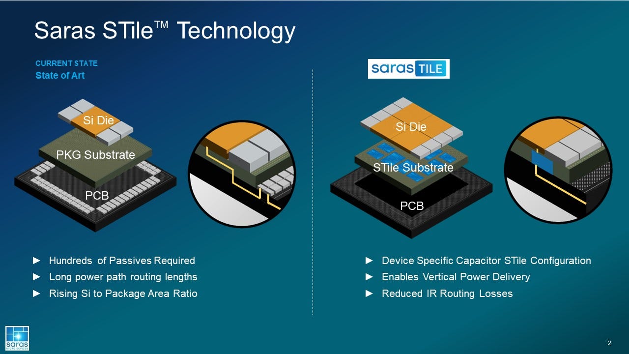
Semiecosystem: How does STile work? Where does it fit in the package?
Bergman: Our initial STile product is a custom configured, multi-domain capacitive module that’s designed to be embedded in the substrate core. We work with our customers to understand their passive device requirements and then design and manufacture the STile to comply with their layout and performance specifications. There are several benefits to our integrated STile design approach. Certainly, one of paramount significance is the provision of a known-good module, which will include high-value components. That will subsequently be embedded into the substrate core. The embedded module enables the relocation of the numerous decoupling/filtering capacitors that currently reside on the package surface, where increasingly there is less space available due to the growing die area into the substrate core. Our STile, in combination with the power management device located on the bottom side of the substrate and the load device on the top side, enables true vertical power delivery. There is already a trend towards embedded passives, but our STile architecture significantly simplifies this approach for both the designer and substrate manufacturer, and results in better performance and reduced substrate yield risk due to the embedding process. The other key point I want to mention is that Saras’ capacitor technology is not based on traditional MLCC (multilayer ceramic capacitor) structures. The capacitor device integrated into our modules was internally developed and has demonstrated significantly better capacitive stability under bias and elevated temperature than competing solutions, both of which are critical for embedded applications.
Semiecosystem: Can you comment on your roadmap?
Huemoeller: Saras is already, in parallel, actively developing the next generation of our STile product line, with immediate focus on AI devices, which will integrate both internally developed capacitor and inductive structures to support embedded voltage regulation. We are targeting to demonstrate initial proof of concept prototypes early next year and plan to introduce an IVR STile product to the industry in the second half of next year. In addition, we’re continuing to advance our capacitor technology to enable even higher capacitive densities and a broader frequency response.
Bergman: Continue to keep an eye on us as we address and deliver AI power issues with STile.
Source: Company