
Intel Unveils Chiplet Alliance To Enable New Chip Designs
The group will help pave the way towards a new class of chips

By Mark LaPedus
At its recent foundry conference, Intel officially announced the formation of a new group that will help propel the development of a technology called chiplets.
The new group, called the Chiplet Alliance, includes Intel, Ansys, Arm, Cadence, Siemens, Synopsys and others. The group will help pave the way towards a new class of chip designs using the chiplets approach.
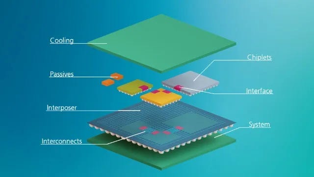
Basically, chiplets are small modular dies or chips, which have a specific function. The dies, or chiplets, are connected and then combined in a package, creating a completely new and more complex chip (See image below). This approach is a fast and low-cost way to develop complex chips, but there are several challenges to develop them.
The chiplets approach is a different way to develop new and advanced chips. This approach isn’t new and the concept has been around for some time. But recently, chiplets have been gaining traction, and for good reason: In some cases, the traditional way of developing high-end and complex chips is becoming too difficult and expensive.
Traditionally, for high-end applications, chip vendors have developed various types of leading-edge and complex devices, such as ASICs and system-on-a-chip (SoC) designs. Generally, these devices integrate all of the components and functions on the same die. This approach works and is still being used today. But the die sizes for many of these complex chips are becoming too large and unwieldy. And in some cases, it has become too expensive to design and manufacture large and complex chips.
That’s where chiplets fit it. In chiplets, you first define and design a complex chip. But in the chip design, you don’t integrate all of the components and functions on the same die. Instead, in the chiplets approach, you may have an assortment of small and modular dies, or chiplets, in an IP library on a computer. Each chiplet performs a specific function. And each chiplet could be manufactured using a different process.
Nonetheless, from the IP library, you select the chiplets that will be used to create the new chip design. Then, you take the chiplets and partition them as defined by the design. From there, the chiplets are electrically connected using die-to-die interconnects, enabling the dies to communicate with each other. Finally, the chiplets are assembled into a package.
In one example, let’s say you want to develop a chiplet-based processor for the data center. In this case, you select various chiplets, such as processor cores, memory controllers and I/O. Then, you combine the chiplets, connect the dies, and put them in a package, creating a new chiplet-based processor.
Using this approach, you have developed a new and functional chip or even an SoC-like device. This chip incorporates several different chiplets within the same unit, but it acts as though it is one chip. The chiplet-based design functions like a traditional SoC. What’s more, this approach has several advantages over the traditional methods. It can speed up the design cycles, while reducing the cost. Plus, smaller dies are easier to fabricate than larger dies.
The ultimate goal among the proponents of chiplets is to develop a third-party marketplace. The marketplace would consist of multiple chiplets and reusable IP from different vendors. Then, you can go to this marketplace and mix-and-match different chiplets to create a design.
This sounds like a good idea, but the chiplet marketplace concept doesn’t exist today. That could take several years to develop. In addition, there are several challenges to develop today’s chiplet-based designs. Moreover, the chiplets approach is ideal for high-end and complex devices, but it is too expensive and overkill for most chips. In other words, the chiplets-based approach isn’t a mainstream technology.
Still, the chiplets approach is a viable technology for some applications. Over the years, several companies have developed chiplets-based devices. To broaden the adoption of chiplets, the industry needs to address several challenges with the technology.
In response, Intel’s new Chiplet Alliance and others are addressing the challenges. And with help from its partners in the new group, Intel could make it easier to enable new chiplet-based designs. Intel’s foundry unit is positioned to support customers across the entire chiplet supply chain.
Chiplets allow the integration of various functional units in different technologies on a substrate or into a 3D chip structure. Source: Fraunhofer IIS/EAS
Why chiplets?
The concept behind chiplets isn’t new. Over the years, AMD, Apple, Intel, Nvidia and others have developed chiplet-based devices. Several companies are working on chiplets in R&D.
The chiplets-based approach is a different way to develop a complex chip, as compared to the traditional methods. Traditionally, a company would develop a high-end ASIC or SoC. All of the components and functions are integrated on the same monolithic die.
At some point in the future, a company would like to develop a new and more advanced version of the ASIC or SoC. So to advance the device, the company would cram new and more complex functions on the same die. Over time, the die size of the chip would inevitably become too large. And in some cases, it has become too expensive and difficult to fabricate large chips in the fab.
The traditional approach still works for many devices. But for some time, the semiconductor industry has been looking for new and different ways to develop complex chips.
The chiplet approach is one option. “In contrast to traditional chips, chiplets are small, modular chips that, when connected, form a complete system-on-chip (SoC). They can be likened to high-tech versions of Lego blocks,” said Emily Yan, product manager from Keysight, in a blog. “This approach offers numerous advantages, including enhanced performance, reduced power consumption, greater design flexibility, and cost savings. For instance, when designing a 10mm x 10mm chip in 3nm technology, cutting it up into four or five chiplets, most of them in a previous process node – the cost is lower than its monolithic equivalent. This means engineers can design complex chips more cost effectively and reuse IPs across different process nodes.”
In 2018, AMD made a major breakthrough in the arena. At the time, the company introduced the first processor to feature a chiplet-based x86 CPU design. AMD used the chiplets approach to develop its second-generation EPYC server processor, built around its Zen 2 core architecture.
AMD’s new CPU architecture incorporated several chiplets in what the company called a hybrid multi-die package. The package incorporated eight AMD CPU dies as well as memory controllers and I/O. The CPU dies were based on a 7nm process from TSMC. The memory controllers and I/O were integrated on a separate die, which was based on a 14nm process. The different dies were connected using AMD’s propriety interconnect technology, dubbed the Infinity Fabric.
AMD’s chiplet-based architecture enabled the company to develop a new class of high-performance processors. “The EPYC 7002 Series doubles the maximum number of CPU cores per socket, increases cache memory and doubling both the Infinity Fabric and PCIe bandwidth to support the additional processing capability, all by using an innovative hybrid multi-die packaging approach,” according to TIRIAS Research, in a white paper in 2019.
Since then, AMD has incorporated chiplet-based architectures across its product portfolio. This shift has allowed the company to accelerate the time-to-market with high-performance, energy-efficient and cost-effective chips.
Others have also jumped on the chiplet bandwagon. For example, in 2022, Intel released a GPU line for the data center. The GPU, codenamed Ponte Vecchio, is a chiplet-based architecture, comprising of 47 functional tiles, or chiplets, on five process nodes. The design operates like a single monolithic SoC.
Meanwhile, Nvidia is currently shipping Blackwell, a new GPU architecture for AI applications. The architecture consists of two GPU dies, which are connected using a 10TB/s link. This architecture makes use of eight high bandwidth memory (HBM) stacks. All of these devices are assembled in TSMC’s 2.5D packaging technology, dubbed Chip-on-Wafer-on-Substrate (CoWoS).
How to develop chiplets
There is no single way to develop a chiplets-based design. Each company will likely have its own design and manufacturing process flow. In most cases, the first step is to define a new chiplets-based chip architecture for a specific application. You also need to decide which chiplets and package design are involved here.
From there, the chiplets-based design requires a comprehensive design workflow using various EDA tools. According to Siemens, here’s one possible design workflow:
*Architecture
*Verification
*Place and route
*Electrical analysis
*Mechanical integration
*Thermal and stress analysis
*Design-for-test and test
That’s only the design phase. The chiplets must be manufactured in a fab and then assembled into a package. Here’s a simplified version of the manufacturing flow:
*Select a manufacturing partner or partners (This should be done before the design phase.)
*The individual chiplets are fabricated in a fab
*During the manufacturing process, each chiplet is screened for defects
*After the chiplets are fabricated, the dies are tested
*The chiplets are assembled in a package
*The design is tested
Chiplet challenges
Clearly, designing and manufacturing a chiplet-based design is a complex process. It takes several key technologies--and a lot of resources--to develop a chiplet-based design. AMD, Intel and Nvidia have the resources in-house to develop this product. Most companies don’t have the resources.
Here are some of the other challenges with chiplets:
*Limited set of applications
Not all chips require the chiplets approach. It’s too complex and expensive for most chips. But there are a set of applications that can take advantage of the chiplets approach. For example, large chip designs, such as AI devices and processors, are ideal for chiplets.
*Design challenges
Designing a chiplets-based product is not a simple task. For example, in the design, you need to connect the various chiplets using die-to-die interconnects.
This presents a major challenge. “One of the barriers has to do with the demarcation or interfaces, both in hardware and software,” said Navid Shahriari, executive vice president at Intel, during a briefing at the company’s recent foundry event. “So that’s the die-to-die topologies and die-to-die interfaces. There has been a lot of progress made with interfaces like UCIe (Universal Chiplet Interconnect Express) in this space. But you also need to understand how you have interoperability with clocking, interops and everything else, as well as the physical interfaces. I would say this is one of the biggest items that needs to be dealt with.”
*Risk factors
Developing a chiplet-based product is expensive. To get a return on investment, you need to design a product that generates a lot of sales in the marketplace. But there is no guarantee that the product will succeed. That’s why many companies in the risk-adverse semiconductor industry will avoid using a new approach like chiplets.
*Complex ecosystem
To develop a chiplet-based design, you need several key technologies. You need the right EDA tools. Then, you need a manufacturing and chip-assembly strategy. The chiplet ecosystem is too complex and expensive for most.
*Proprietary technologies
In a chiplet-based design, the chiplets must communicate with one another. Typically, for their respective chiplet-based designs, semiconductor vendors tend to use proprietary die-to-die communication protocols and interfaces. Larger companies can afford to develop proprietary die-to-die technologies. Most vendors don’t have the resources.
*Standards
Fortunately, the semiconductor industry is developing standard die-to-die technologies for chiplets. The idea is to allow more companies to adopt the chiplets concept using open standards.
In 2022, several companies banded together and announced the UCIe Consortium. This specification covers a standard die-to-die I/O physical layer, die-to-die protocols, and software stacks.
That’s the good news. The bad news is that there are other die-to-die protocol standards in the market. In other words, there is no one die-to-die standard for chiplets.
Standards are important in the semiconductor industry. Take WiFi for example. Chip vendors can easily design WiFi chips based on standards. Without standards, it’s hard for companies to jump on the chiplet bandwagon.
*Lack of plug-and-play chiplets
Ultimately, companies want to go to a third-party marketplace and buy verified chiplets from various suppliers. This type of chiplet marketplace doesn’t exist today. It’s unclear when this will happen.
To enable a chiplet marketplace, chip companies must share their proprietary design and test data with others. Most don’t want to share data with their competitors.
“I see an era where you are reusing chiplets from one place to the other and you can mix or match them. But we are still a few years away from that,” Intel’s Shahriari said.
The solutions
It’s not all doom and gloom. As stated, several companies have developed chiplet-based designs. And more products are in the works.
Plus, several foundry vendors, such as Intel and TSMC, have several capabilities in-house to enable the development of chiplets. The outsourced semiconductor assembly and testing (OSAT) vendors, such as ASE, Amkor and NHanced Semiconductors, also have various in-house capabilities for chiplets.
Last year, for example, ASE extended its advanced interconnect technology under the company’s VIPack platform to meet the accelerating demand for complex chiplet integration for AI applications. ASE’s technology allows designers to select various high-density chiplet integration options.
In another example, Intel’s Chiplet Alliance is focusing on the ecosystem to drive interoperable and secure chiplet implementations across a wide range of government and commercial applications.
Intel has devised an extensive ecosystem for chiplets. The partners in the program were chosen for their experience with chiplet design, EDA tools, and IP for seamless in-package communications between chiplets.
Besides Intel, the other members of the group include Ansys, Arm, Arteris, Cadence, Capgemini, Draper, eMemory, HCLTech, Keysight, QuickLogic, Siemens, Synopsys, and Trusted Semiconductor Solutions.
Intel’s foundry unit will provide manufacturing services here. UMC, which is also part of the group, will contribute its foundry experience, diverse process technologies and capacity. “As interest in modular, chiplet-based architectures continues to grow, closer collaboration is essential to help customers harness the performance, energy efficiency and cost benefits of integrated multi-die solutions,” said GC Hung, senior vice president of technology and business development at UMC.