


Japan’s Rapidus Preps 2nm Foundry Process And Chiplets
An executive from the Japanese foundry startup discusses the company’s strategy, including its efforts to develop a 2nm gate-all-around (GAA) process.

By Mark LaPedus
Henri Richard, general manager and president of Rapidus Design Solutions, sat down with Semiecosystem to discuss the company’s foundry strategy and its efforts to develop its first process--a 2nm gate-all-around (GAA) technology. Rapidus Design Solutions is the U.S. subsidiary of Japanese foundry startup Rapidus Corp.
Semiecosystem: Who is Rapidus and what is the company’s charter?
Richard: Rapidus is a Japanese semiconductor foundry established by 14 semiconductor experts, including two veteran semiconductor executives, Dr. Atsuyoshi Koike, CEO, and Tetsuro Higashi, chairman of the board. Rapidus’ founding mission is to establish Japan as a leading provider of logic semiconductor foundry services. We’re completing the construction of our advanced Innovative Integration for Manufacturing (IIM-1) foundry in Chitose, Hokkaido with the support of the community, government and local universities.
Semiecosystem: Where is your fab located and what is the status of your fab? And what are the company’s capital spending plans for 2025 and perhaps beyond?
Richard: Rapidus IIM-1 is a ‘mega fab’ conveniently located a few miles from the New Chitose International airport. To give a sense of the scale, the project site is larger than Disneyland Japan with the fabrication clean room larger than the Tokyo Dome. IIM-1 is scheduled to start pilot production in April 2025. The fab will integrate both front-end and back-end capabilities to provide customers with best-in-class turnaround time and optimized engineering for manufacturing feedback.
Semiecosystem: Can you discuss your roadmap? Who is your technology partner?
Richard: The first node will be based on a high-performance GAA 2nm technology developed by IBM in Albany, N.Y. We are now developing mass production technology together with IBM, having dispatched over 150 engineers from Japan to Albany.
Semiecosystem: Will Rapidus integrate a backside power delivery network (BSPDN) technology for the first version of your 2nm GAA process? Or will you bring up BSPDN later?
Richard: BSPDN will be provided shortly after the start of our mass production in 2027 and is an integral part of the roadmap going forward.
Semiecosystem: Why does the semiconductor industry need another leading-edge foundry vendor? Is there room for another vendor like Rapidus in the marketplace? After all, TSMC provides a large percentage of the world’s leading-edge foundry business. Samsung also competes in this segment with Intel waiting in the wings.
Richard: The current surge of AI-based applications is creating an unprecedented demand for leading-edge semiconductors. Beyond the geopolitical challenges, the industry is desperately in need of more capacity from a diversified supply chain and a streamlined foundry process. Rapidus is ideally positioned to address the main concerns of any company needing a new partner in the foundry business.
Semiecosystem: Years ago, Japanese semiconductor companies were among the leaders in both logic and memory technology. With Kioxia, Japan has a strong presence in NAND flash memory. But today, Japan appears to be behind in logic—its most advanced logic technology is 40nm. So, I assume that Rapidus is important in terms of national security for Japan’s semiconductor industry, right?
Richard: Semiconductor logic manufacturing has become a strategic capability for any nation wanting to participate in advanced AI-based technologies. Japan’s long history in both logic and memory manufacturing, along with its strong contribution to the world of advanced semiconductor equipment and materials, enabled Rapidus to secure public and private sector support while attracting a new generation of engineering talent to work with one of Japan’s flagship projects.
Semiecosystem: Intel, Samsung, TSMC and others have been working on GAA for many years. GAA provides more performance at lower power than today’s finFET transistor technology. GAA shares many of the same process steps as finFETs. Yet, GAA is a difficult technology and a challenge when ramping up high yields. With that in mind, there is some skepticism among many that Rapidus will be able to bring up GAA technology into production promptly. Rapidus has no track record in chip manufacturing. Any comments here?
Richard: GAA is the perfect technology inflection point for Rapidus to enter the market. Everyone in semiconductor logic manufacturing is facing similar challenges converting from finFet to GAA technology. We have the benefit of being able to start with the most advanced equipment, integrate several industry-first innovations and heavily apply AI analysis to the manufacturing data to optimize the cycles of learning. Through a strategic partnership with IBM, which developed GAA technology, we are designing technology for mass production. It is one big advantage. In addition, our single wafer processing method provides us with a significant advantage in turnaround time that will translate into industry leading yield curves and overall productivity.
Semiecosystem: What are some of the main technical challenges with GAA?
Richard: While GAA technology presents exciting opportunities and benefits over finFET, as any innovative technology, it will have areas that will require careful attention. We are building the necessary capabilities to effectively address potential challenges including:
*Advanced material engineering techniques to enhance the reliability and performance of the interlayer dielectrics for increased device efficiency.
*Precision manufacturing using state-of-the art equipment and materials, AI and automation for achieving the highest level of process control, fast optimization and consistent process performance.
*While initial costs may be high, the integration of GAA technology leads to significant long-term savings through improved power efficiency and performance. Our objective is to drive cost efficiencies with our advancements in manufacturing processes and accelerate turnaround times.
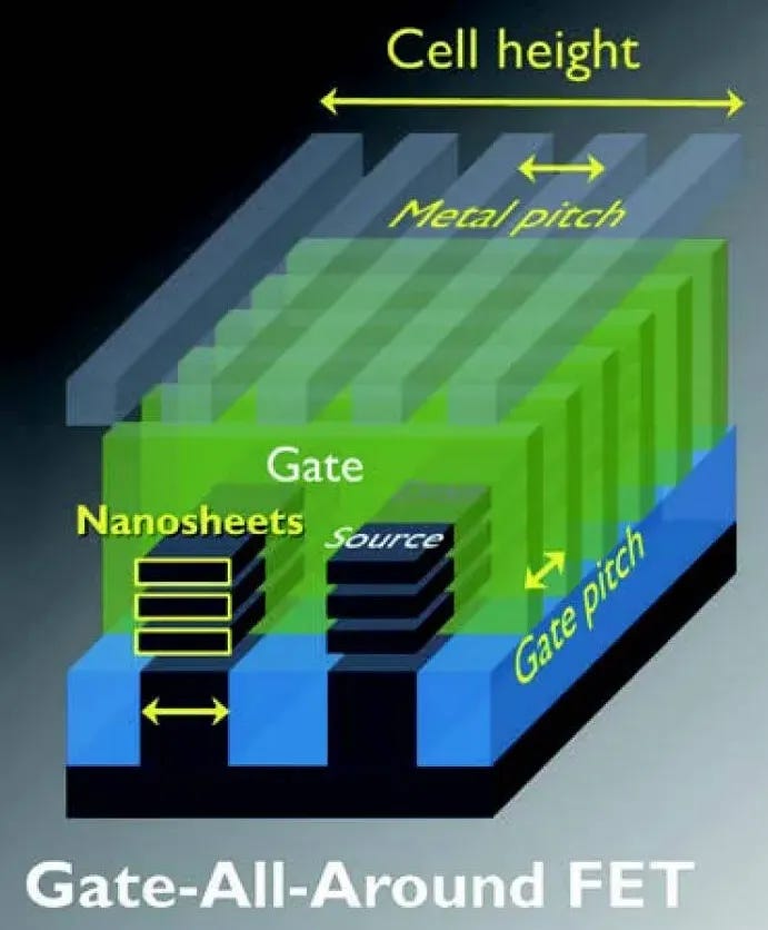
Rapidus’ 2nm process will use a gate-all-around (GAA) transistor structure, which will deliver high-performance and low-power chips. Source: Company
Semiecosystem: The foundry business is also challenging. For one thing, a given foundry vendor must ramp up a given process on time. Then, a foundry vendor must find customers and develop a certain level of trust with those customers. Then, a foundry must deliver chips to customers on time with good yields. Rapidus is a newcomer here. Why should potential foundry customers work with Rapidus? What are the company’s competitive advantages?
Richard: Rapidus is offering our future customers several dimensions of differentiation. Located in a geopolitically favorable country, Rapidus will offer best-in-class turnaround time, the most advanced integration among design solutions, front-end and back-end process development, and very high manufacturing flexibility.
Semiecosystem: Foundries also require an EDA and IP ecosystem. How far along is Rapidus in developing this ecosystem?
Richard: Rapidus recently announced agreements with both Cadence and Synopsys, and we are working on additional ecosystem partnerships.
Semiecosystem: Rapidus has developed a technology called RUMS (Rapid and Unified Manufacturing Service). What is RUMS and what are the benefits?
Richard: RUMS provides a seamless integration of design solutions and front-end and back-end processes, ensuring efficient and cohesive semiconductor production. By optimizing design and manufacturing processes, RUMS significantly reduces the overall time-to-market for semiconductor products, which will allow our customers to bring their products to market faster. In the design solution area, RUMS incorporates AI-driven design optimization tools, such as Rapidus AI-Assisted Design Solutions (Raads) to enhance design efficiency and accuracy. RUMS offers an extensive support for design, manufacturing and system integration, providing customers with a holistic solution that addresses all aspects of semiconductor manufacturing.
Semiecosystem: Rapidus will also provide customers with packaging technology, right? What is Rapidus Chiplet Solutions (RCS) and what does that involve?
Richard: Rapidus Chiplet Solutions (RCS) is our R&D and pilot line focused on advanced semiconductor packaging and chiplet integration technologies. It is in a state-of-the-art facility within Seiko Epson’s Chitose campus in Hokkaido, Japan, and walking distance from our IIM-1 facilities.
RCS will focus on the development of our packaging technologies, including flip chip ball grid array (FCBGA), 2.5D Si interposer, organic interposer and redistribution layer (RDL) technologies and 3D hybrid bonding. These technologies are crucial for next-generation high-end applications and chiplet integration.