
Multibeam Debuts Next-Gen E-Beam Lithography Tool
Multibeam introduced its new multi-column e-beam litho tool and received an order for the product

By Mark LaPedus
Multibeam Corp. has rolled out its next-generation multi-column e-beam lithography system and has received an order for the product.
National Tsing Hua University (NTHU) in Taiwan has ordered Multibeam’s new MBX multi-column e-beam lithography system for its College of Semiconductor Research. NTHU will install the system in a new facility to support academic research, as well as joint development projects with Taiwan’s chipmakers.
Based in Sunnyvale, Calif., Multibeam is developing and shipping an advanced form of e-beam lithography. In general, electron-beam lithography, sometimes called direct-write or maskless lithography, is a system that generates a single focused electron beam. Then, the beam patterns the surface of a material or chip on a stage inside the system. All told, e-beam lithography enables fine resolutions, but it is slow.
Multibeam’s new MBX system addresses this issue. The MBX system incorporates an array of miniature e-beam columns. In operation, each mini e-beam column writes patterns in parallel directly on the wafer. Using this multiple beam approach, the system is capable of high-productivity volume manufacturing (See Figure 1).
“That’s the key. Each column is only one beam. Each column is individually controlled, but they write in parallel,” said David Lam, founder, chief executive and chairman of Multibeam.
Multibeam’s new MBX system isn’t exactly targeted for leading-edge logic and memory. Instead, the MBX is targeted for more specialized applications, such as advanced packaging, compound semiconductors, photonics, quantum computing and secure chip ID.
“You need specialty lithography for these emerging areas. This includes photonics, co-packaged optics, quantum and next-generation advanced packaging,” said Ken Macwilliams, president of Multibeam. “Those do not need EUV. It isn’t all about the 1.5-nanometer node.”
In 2010, Multibeam was founded by Lam, a long-time semiconductor executive. In 1980, Lam was also the founder and first chief executive of Lam Research, a supplier of semiconductor equipment. (David Lam is no longer associated with Lam Research.)
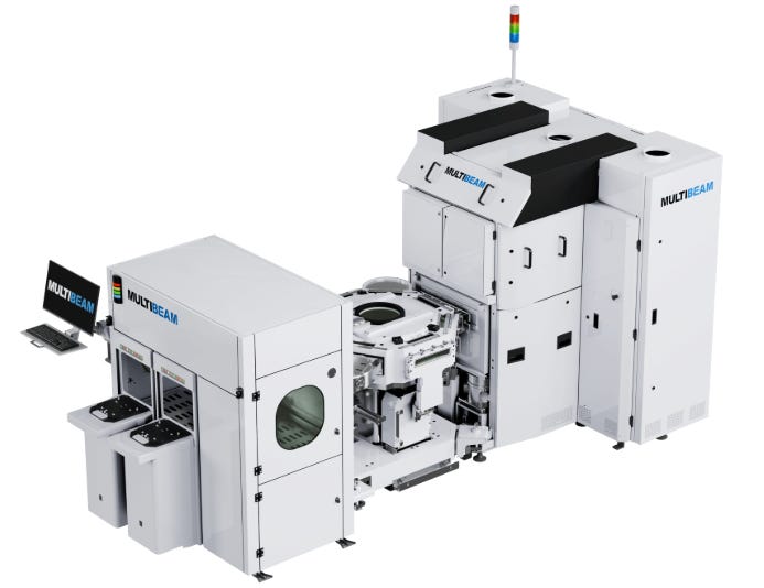
Figure 1: Multibeam’s new MBX Multi-Column E-Beam Lithography system Source: Company
Lithography landscape—optical litho
Before describing Multibeam’s new system, let’s first take a look at the lithography landscape and what role this critical technology plays in chip manufacturing.
Basically, a chipmaker (i.e. Intel, Samsung, TSMC, others) manufactures a multitude of chips using various process steps in a large facility called a wafer fab. Lithography is one of the key process steps in the fab. In a fab, a chipmaker will use lithography equipment to pattern the tiny features in chips. A device will also undergo other process steps in a fab, which in turn creates a finished chip line.
There are various types of lithography equipment in the market, including optical lithography, extreme ultraviolet (EUV) lithography, nanoimprint lithography and e-beam lithography.
Each type is different. Each type is viable and used for different applications. In this article, I will describe each lithography type, including Multibeam’s new system. It’s important to understand where each lithography type fits in the semiconductor landscape.
Let’s start with optical lithography. For years, optical lithography has been the mainstream production system in fabs. In a fab, optical lithography systems are used to pattern both trailing-edge and advanced devices. It is widely used to process various chip types, including analog devices, logic products, memory and power semiconductors.
Optical lithography is fast and reliable. In operation, light is generated inside an optical lithography system. Then, the light is projected through a photomask inside the system. A photomask (or mask) is master template, or blueprint, of the pattern that will be printed on the wafer.
“With the pattern encoded in the light, the system’s optics shrink and focus the pattern onto a photosensitive silicon wafer,” according to ASML, a supplier of lithography tools.
Current state-of-the-art optical lithography tools use deep ultraviolet (DUV) light at 193nm wavelengths. This enables the tool to print feature sizes down to 38nm.
The tool can also produce smaller features. Using complex multiple patterning techniques, a 193nm immersion optical lithography system can pattern chips down to the 7nm process node. Beyond the 7nm node, optical lithography becomes too unwieldy and complex.
Lithography landscape—EUV
To manufacture chips at the 7nm process node and below, chipmakers use EUV lithography. ASML of the Netherlands is the sole supplier of EUV lithography scanners in the market. EUV lithography uses light with a wavelength of 13.5nm. With a numerical aperture (NA) of 0.33, EUV scanners print features in chips at 13nm resolutions.
Today, Intel, Samsung and TSMC are using EUV lithography to produce logic chips (i.e. AI chips, processors, etc.) at the 5nm, 3nm and 2nm process nodes. Micron, Samsung and SK hynix are using EUV for advanced DRAM production.
EUV is expensive. A 0.33 NA EUV lithography tool sells for $180 million—each. EUV lithography also requires a complex and expensive mask.
ASML is also developing a next-generation EUV technology called high-numerical aperture (High NA) EUV. A High NA EUV scanner incorporates a 0.55 NA lens, enabling 8nm resolutions. High NA is also expensive. Each tool sells for a staggering $400 million.
Still, Intel has put High NA EUV into production. Micron, Samsung, SK hynix and TSMC are still evaluating the technology.
Lithography landscape—nanoimprint, e-beam litho
Besides optical and EUV, there are other types of lithographic equipment, such as nanoimprint and e-beam.
“Nanoimprint lithography (NIL) equipment forms patterns on wafers by pressing a mask containing circuit patterns into resist in an imprint process,” according to Canon, a supplier of NIL tools. “Unlike conventional lithography technology that uses light to expose circuit patterns, NIL does not require a light source.”
Canon’s NIL steppers provide ≤15nm resolutions. In general, the drawback for NIL is overlay. NIL is mainly used for niche-oriented applications.
Traditional e-beam lithography, meanwhile, has been around for several decades. E-beam lithography scans a focused beam of electrons to directly pattern a surface. E-beam lithography is a maskless technology. It doesn’t require a photomask, which reduces the cost-of-ownership.
Typically, e-beam lithography uses a single beam of electrons, enabling fine resolutions. For example, RAITH, a supplier of fab equipment, sells an e-beam lithography tool with resolutions below 5nm. The system features a 100kV column with automated exposure parameter switching and calibration. This allows the system to switch between high-throughput and high-resolution modes.
But single-beam e-beam lithography is slow. Thus, the technology is not used for high-volume mainstream chip production. Instead, e-beam lithography is ideal for specialized applications, such as compound semiconductors, optoelectronics, photonics and quantum computing. It is also ideal for R&D labs and universities.
Multibeam’s approach
Meanwhile, Multibeam’s multi-column e-beam lithography (MEBL) system is also a direct-write lithography system. But it is different than traditional e-beam lithography tools. Multibeam’s system addresses the productivity challenges in device production. Like traditional e-beam lithography, though, Multibeam’s tool is also maskless.
Multibeam’s previous tool was a 200mm system with 80nm resolutions. In contrast, Multibeam’s new MBX system has a lot more capabilities. The new tool supports 3-inch, 4-inch, 6-inch, 8-inch and 12-inch wafers. It also supports 310mm x 310mm panels for advanced packaging.
The new system also supports silicon wafers and glass substrates. It also handles various compound semiconductor devices, based on gallium nitride (GaN), indium phosphide (InP) and silicon carbide (SiC).
The automated system supports up to three writing chambers. It has resolutions from over 1µm down to 30nm and below. It provides 10X the productivity over single-beam e-beam lithography tools.
Multibeam’s throughput advantage stems from a multiple-column architecture. Each tool can incorporate some 18 individual and miniaturized e-beam columns. In operation, each column writes independently and in parallel for maximum productivity.
“Each mini e-beam column self-calibrates, self-aligns, and independently writes patterns with high resolution and precision,” according to a recent paper from Multibeam and Deca. “MEBL further enhances productivity by writing nonstop while the stage is in motion, offering an additional ≈5X throughput advantage due to the ‘write-on-the-fly’ capability. Moreover, MEBL employs a reduced acceleration voltage (up to 10X lower than a conventional system), which directs more of the electron’s energy towards exposing the resist, rather than heating the substrate, providing an additional throughput advantage.”
As stated, the MBX is targeted for more specialized applications, including advanced packaging, compound semiconductors, photonics, quantum computing and secure chip ID.
New order
In recent times, Multibeam shipped one of its systems to Skywater Technology, a U.S.-based foundry vendor. Now, Taiwan’s NTHU has ordered Multibeam’s multi-column e-beam lithography system for its College of Semiconductor Research. The shipment planned for 2027.
The tool will train the next wave of engineers in Taiwan. “Our mission is to accelerate the development of next-generation semiconductor technologies for rapidly growing applications like advanced packaging, photonics and quantum computing,” said Burn Lin, Distinguished Research Chair Professor at NTHU.
In 2021, NTHU established the College of Semiconductor Research. The college provides classes in device physics, advanced technologies and other topics. Lin has held various positions at IBM and TSMC. At IBM, Lin spearheaded the development of immersion lithography. From 2000 to 2015, he held various positions at TSMC.
“NTHU is an outstanding partner for our first order from Taiwan. With infrastructure technologies like AI catalyzing new IC manufacturing innovations more rapidly than ever, the university leads by pioneering novel processes that can be transferred swiftly to production,” Multibeam’s Lam said.