

By Mark LaPedus
In case you missed it, Elon Musk recently announced plans to build a new and giant fab.
The fab project, called Terafab, is a joint effort between Tesla and SpaceX. Musk’s goal is to build a large semiconductor fab in Austin, Texas--at a cost of $20 billion to $25 billion. A fab is a large facility used to manufacture chips.
If Musk makes good on his promise, the Terafab will manufacture chips for Tesla and SpaceX. The proposed Terafab is expected to manufacture both logic and memory chips all in the same facility. Initially, the goal is to produce logic chips at the 2nm node. And if that isn’t enough, the same facility will also package and test these chips.
The production date is still unclear. Some speculate that pilot line production could start in 2028. There is also a possibility that the fab will never get off the ground, and for good reason: The company has no experience in building and operating a fab.
Musk, chief executive of Tesla, has been talking about the Terafab for several weeks. Initially, Musk’s fab plans were met with some skepticism. That hasn’t changed, and for good reason: Some of the goals and claims for the Terafab project don’t quite add up and are simply unrealistic.
Musk, the world’s richest person, certainly has the resources to build the Terafab. But he faces numerous challenges in getting a semiconductor fab off the ground. It’s an expensive and difficult endeavor.
So, the question is clear: Is the Terafab real or not? Right now, the Terafab is a still a “PowerPoint” presentation. Of course, that could change. To make it real, we would need to see the fab at action, churning out chips in volumes.
Still, Musk’s Terafab is worth exploring. Here, I will analyze the Terafab announcement and will answer the following questions:
*What is the Terafab?
*Why build the Terafab?
*What’s missing in the fab announcement?
*What are challenges to build a fab?
*Can the Terafab keep up with TSMC?
*Should Musk even build a fab?
I provide an analysis for each question in detail below.
What is the Terafab?
Based on Musk’s vision, the Terafab is expected to become one of the world’s largest fabs with 100 million square feet. The Terafab is expected to handle all aspects of the semiconductor production process all in the same facility, including:
*Photomask production
*Logic and memory chip production
*Packaging and test
The fab is expected to manufacture two types of chips—rad-hard products and AI devices. First, the fab is expected to make radiation-harden chips for space applications. Second, the Terafab is expected to manufacture AI edge inference chips. These AI chips would be used for Tesla’s electric vehicles (EVs) and self-driving cars. These chips would also be used for Optimus, the company’s general-purpose humanoid robot line.
Reports have surfaced that the fab will initially produce chips in late-2027. That’s unrealistic. Others say pilot line production could start in 2028.
Here’s my assessment (and opinion) here:
*There is a zero percent chance that the Terafab will move into production by 2027/2028.
*There is a 20% chance that the Terafab will move into the pilot line phase by 2029.
*There is an 80% chance that the Terafab will never happen. The company has no experience building and running a fab. Generally, the goal is to keep a fab utilized with large chip volumes. It’s difficult to see how the company will keep the Terafab even remotely utilized with rad-hard and AI edge chips.
Nonetheless, for now, the Terafab appears to be a captive fab. In other words, the fab will mainly manufacture chips for Tesla and SpaceX. Musk has not positioned the Terafab as a foundry vendor. The fab is not expected to manufacture chips for other companies, at least for now. So, the Terafab will not compete against Samsung, TSMC and other foundry vendors.
If Musk actually builds the Terafab, the company (Tesla/SpaceX) would be considered as an integrated device manufacturer (IDM). An IDM is a vertically integrated semiconductor company. IDMs have the means to handle everything, including chip design, fab production and packaging.
The IDM model isn’t new--it’s been around for ages. Today, several semiconductor companies--such as Intel, Micron, Samsung and Sk Hynix—are IDMs to one degree or another.
Typically, IDMs design their own chips and then sell them on the open market. IDMs also manufacture their chips within their own fabs. Generally, these fabs are situated in different locations and countries.
That way, IDMs can spread the risk, and, in some cases, reduce the cost. For example, packaging is a labor-intensive endeavor. IDMs tend to put their large-scale packaging plants in low-cost regions in Asia.
Musk, meanwhile, is putting a new twist on the IDM model: He wants to put everything in the same location and under the same roof. That makes sense from a supply chain perspective, but is that even possible?
That’s entirely possible based on the proposed design of the fab. The Terafab is expected to be modular. It includes 10 separate modules, according to “Not a Tesla App,” a Tesla enthusiast site that closely follows the company.
In theory, each module could handle a separate process. Then, in the fab, the Terafab plans to implement a fast recursive loop for improving chip designs.
Others are also developing this AI-based chip design methodology. For example, Ricursive Intelligence, a startup based in Palo Alto, Calif., is building a next-generation platform that uses AI to accelerate and optimize every stage of the chip design process, creating what it calls a recursive feedback loop: “AI models design the next generation of chips and those chips, in turn, train more advanced AI models,” according to Ricursive Intelligence.
All told, the Terafab is doable, but it’s still unclear if it will really happen. If it does happen, it’s going to be expensive.
Why build the Terafab?
Why is Musk building a fab? To answer that question, let’s first take a step back and take a brief look at Tesla, SpaceX and Starlink. Based in Texas, SpaceX is a spacecraft manufacturer. In 2026, SpaceX acquired Musk’s AI venture, dubbed xAI. Starlink is a satellite internet service developed by SpaceX to provide high-speed broadband, especially in remote areas, utilizing a constellation of thousands of low Earth orbit (LEO) satellites.
Tesla is the world’s second largest electric vehicle (EV) maker, behind China’s BYD, according to TrendForce (See chart below). Tesla is also developing Optimus, a general-purpose, bi-pedal humanoid robot capable of performing various tasks.
Tesla is a vertically integrated company. It is involved in many parts of the supply chain, including material sourcing, software development, manufacturing and direct sales.
Tesla and SpaceX can’t do everything. Both entities buy a large number of chips from various semiconductor companies. Tesla, however, designs its own chips for select applications. For example, the company designs the so-called Full Self Driving (FSD) processor chip, which is used to power the self-driving functions in Tesla’s EVs.
Tesla doesn’t own or operate a fab—it relies on foundry vendors. Tesla’s FSD chips are manufactured by foundry vendors, namely Samsung and TSMC. In fact, Tesla last year announced a $16.5 billion foundry deal with Samsung. Under the terms, Samsung will make select chips for Tesla’s EVs.
Meanwhile, the overall car market is stagnant. The EV market continues to grow, but at a much slower pace. In 2026, the battery-electric vehicle market is projected to grow by 19% to 17.4 million units—about 19% of the global vehicle sales market, according to S&P Global Mobility.
In the EV market, Tesla is losing share. The U.S. company faces stiff competition from EV makers from China and elsewhere.
Still, Musk wants more foundry capacity. FSD chips will drive some demand. In the future, Musk says that he needs an enormous amount of chips for the company’s humanoid robot lines. In total, the humanoid robot market is expected to be somewhere between 1 billion and 10 billion units a year, according to Musk.
Robotics have always been the next big thing in the consumer market. For consumers, though, robots are still not ready for prime time. However, there is a place for industrial robots on the factory floor.
Nonetheless, Samsung and TSMC are willing to manufacture a certain amount of chips for Tesla. But beyond a certain point, Samsung and TSMC aren’t willing expand their fab capacities—just for Tesla.
That’s why Musk wants to build the Terafab. “We’re very grateful to Samsung, TSMC, Micron, and others, and we would like them to expand as quickly as they can. We will buy all of their chips—I’ve said these exact words to them,” Musk said during a recent event. “But there’s a maximum rate at which they’re comfortable expanding, and that rate is much less than we would like. So we either build the Terafab or we don’t have the chips. And we need the chips. So we’re going to build the Terafab.”
You can’t blame TSMC, Samsung or Micron here. (Micron is a key memory supplier for Tesla.) These companies not only serve Tesla, but they also produce chips for a large number of other customers.
Tesla is an important customer. But the amount of chips consumed by Tesla is relatively small, compared to other OEMs like Apple. Tesla’s demand pales in comparison to that of Nvidia. Thus, Tesla doesn’t have the leverage to demand more fab capacity from TSMC or Samsung.
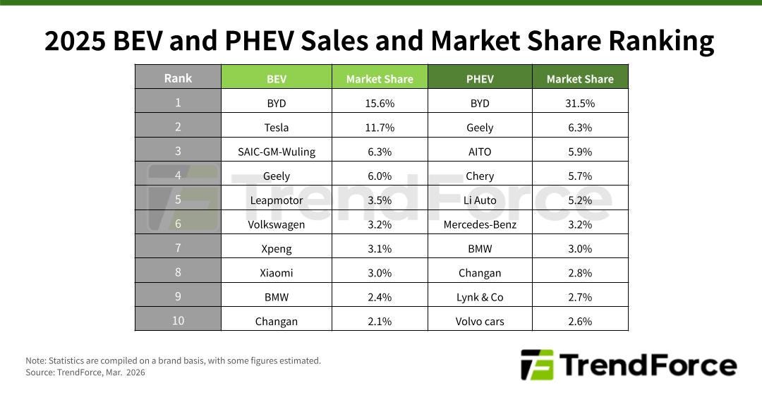
OEM rankings for battery-electric vehicles (BEVs) and plug-in hybrid electric vehicles (PHEVs). In the 2025 BEV rankings, BYD posted approximately 25% YoY growth, overtaking Tesla to claim the top position. Source: TrendForce
What’s missing here?
Meanwhile, there are more questions than answers about the Terafab announcement. For example, in a typical fab introduction, a semiconductor company tends to list the following details: investment amount, fab/cleanroom size, groundbreaking date, and production date.
It’s also important to know what types of chips that are being produced in the fab. Some will also list the monthly wafer starts and how many jobs the fab will create. And if needed, a company will disclose any funding agreements, technology partners or licensing deals.
During the introduction of the Terafab, Musk disclosed few details about the fab. There was no official timetable given regarding the groundbreaking or production dates. Another question: Where is Musk obtaining his logic and memory technology?
Logic (i.e. AI chips, processors) and memory (i.e. DRAM, flash memory, HBM) are different. To produce logic and memory devices in a fab, you need two process technologies—one for logic and another for memory.
Will Musk develop these technologies on his own or will he find technology partners? This remains unclear, leaving some to believe that the Terafab isn’t quite ready for prime time.
What are challenges to build a fab?
Building and running a leading-edge fab is a major undertaking. Given that Musk has formed alliances with TSMC and Samsung, I assume he knows the challenges here.
“A typical fab includes 1,200 multimillion-dollar tools and 1,500 pieces of utility equipment,” according to Intel. “It costs about $10 billion and takes three to five years and 6,000 construction workers, to complete. Three of the fab’s four levels support the clean room, the home to chip production.”
It’s possible to build a fab in two or so years. Today, a leading-edge fab could cost $20 billion or more.
To build a fab, a construction company first builds the shell of the building. Then, the contractor builds a cleanroom and a sub-fab. During that period, a semiconductor company buys the tools, or production equipment, for the fab. Once the building is completed, the tools are installed and hooked up in the finished cleanroom.
Some fab tools must be ordered a year or more in advance. The equipment is also expensive. For example, a leading-edge fab requires ASML’s extreme ultraviolet (EUV) lithography tools. EUV lithography is used to process the world’s most advanced chips. At a starting point, an EUV lithography tool sells for $180 million—each. A next-generation EUV lithography tool, called high-NA lithography, sells for $400 million each.
Once the tools are hooked up in the facility, a semiconductor company develops a process in the fab. A process is the recipe that is used to manufacture a chip line. The goal is to develop a process in the fab, which can produce chips in a timely manner with good yields.
There are several challenges here. At each new process generation, the chips are becoming more complex. For example, today’s advanced chips incorporate billions of tiny structures and complex materials in the same device. The feature sizes of these structures can be measured down to the nanometer, or angstrom, range.
Thus, the chips are becoming more difficult and expensive to manufacture in the fab. Plus, in the fab, an advanced chip may undergo 1,000 process steps or more during the flow.
At times, there might be a glitch in the process. A glitch could cause unwanted defects in a chip line. A chip riddled with defects may result in a faulty part. That chip could fail in the field.
So, if there is a glitch in the process, it’s important to fix the problem. That takes time and money.
All told, it’s important to develop a sound process in the fab from the beginning. That’s just the starting point. The process must be qualified, ensuring that the flow will produce the desired chips with good yields.
It’s also important to run test chips in the fab. That will determine whether the chip works and meets spec. If the test chips have poor yields or too many defects, there might be an issue with the process, the fab tools, or the chip design itself. In any case, it’s important to find the problem and fix it. But at times, locating the problem is like finding a needle in a haystack.
Finally, if all goes well, the chips are put into production. That’s a simple way to describe a complex process.
That takes longer than a year, even for the most experienced chipmakers. Thus, it’s difficult to believe that the Terafab will move into pilot line production in 2027/2028. It’s more like 2029/2030—if at all.
Can the Terafab keep up with TSMC?
Generally, today’s leading-edge chipmakers, namely Intel, Samsung and TSMC, are introducing a new full-node process roughly every 24 to 36 months.
Then, at roughly the same interval, some companies are introducing new chips, which are manufactured using the latest processes. With these new processes, the chips are becoming faster with more functions at each turn.
At each new process generation, a chipmaker needs to invest in new fabs, processes and equipment. It’s expensive. TSMC’s 2026 capital spending budget is expected to be between $52 billion and $56 billion. In 2025, TSMC spent $40.9 billion, as compared to $29.8 billion in 2024.
The Terafab hopes to produce leading-edge chips, but can it keep pace with Intel, Samsung and TSMC?
Let’s say the Terafab can manufacture chips at the 2nm node. And let’s pretend that the Terafab moves into pilot line production by 2028. In this hypothetical scenario, the fab would enter into volume production by 2029/2030.
At that point, the Terafab would already find itself at least three to four years behind the curve. 2nm is already in production. In late 2025, Intel, Samsung and TSMC separately began to ramp up their respective 2nm-class processes in the market.
Then, by 2028, TSMC is expected to release its A14 (1.4nm) process. A14 represents TSMC’s second-generation gate-all-around transistor technology. Beyond A14, TSMC is working on other advanced processes.
In other words, TSMC and others will continue to develop new processes at a rapid pace. The Terafab will have a difficult time keeping up. Tesla can ill afford to be three to five years behind in process technology.
So, for the foreseeable future, Musk may need to rely on foundry services from TSMC and Samsung for its advanced chips, leaving many to wonder: Why build the Terafab in the first place?
Should Musk build the fab?
So, the big question is clear: Should Musk even build the fab? Before answering that question, here’s what Tesla/SpaceX should focus on in numerical order:
1—Tesla is losing share in EVs. It should focus on regaining share.
2—Tesla is behind in robotaxis. Humanoid robots too. Among more than 300 humanoid robot enterprises worldwide, China is leading the market, according to Counterpoint Research. It’s time to play catch-up.
3—SpaceX should focus on future moon missions. Maybe Mars too.
Building a fab should be the last priority. It’s expensive and a drain on resources. It won’t generate any revenue. It could drag the company down.
But let’s say Musk moves ahead with the Terafab. If so, he should:
1—Hire a seasoned foundry CEO. Let the CEO call the shots. (Non-foundry execs won’t work.)
2--Hire experienced fab workers
3--Find technology partners (i.e. IBM, Imec, Intel)
4—Stay out of the memory business. It’s too difficult. Continue to source from Micron and others. License embedded flash, MRAM and ReRAM from third parties.
5—Set up a packaging venture with an experienced player. Packaging is a different mindset.
6—Take a more traditional approach to chip production. New approaches are probably needed, but they are too risky. Still, there is always room for innovation and new breakthroughs. As before, it comes down to cost. The goal is to make better chips at lower costs. If you can do it better, then it’s time to break ground.