
NXP, Onsemi Go Different Directions In GaN
And at IEDM, several entities presented papers on the latest R&D breakthroughs in GaN

By Mark LaPedus
Two major semiconductor companies—NXP and onsemi—are moving in different directions in the gallium nitride (GaN) device market.
On one hand, NXP, a Dutch-based semiconductor supplier, plans to wind down its radio power product lines, including its GaN-based devices. In addition, NXP plans to shutter its GaN fab in Arizona.
On the other hand, onsemi, a U.S.-based chip supplier, is expanding its efforts in the GaN semiconductor market. In recent times, onsemi has signed separate GaN deals with China’s Innoscience and U.S.-based GlobalFoundries.
Others are also expanding their efforts in GaN. And at the recent IEEE International Electron Devices Meeting (IEDM) in San Franciso, several entities presented papers on the latest breakthroughs in R&D for GaN.
What is GaN?
GaN, a III/V compound that combines gallium and nitrogen, is a hot topic. GaN is a wide bandgap (WBG) semiconductor material. “A ‘bandgap’ is the amount of energy needed to release electrons in semiconductor materials so that the electrons can move freely—allowing electricity to flow,” according to PowerAmerica, a U.S.-based power semiconductor consortium.
WBG semiconductors have bandgaps that are greater than traditional silicon-based chips. Silicon has a bandgap of 1.1 eV, while GaN is 3.4 eV. Silicon carbide (SiC), a WBG material, has a bandgap of 3.3 eV. Gallium oxide, which is in R&D, is 4.8 eV (See chart below).
“GaN is a compound semiconductor material used to create high-performance power devices known as GaN HEMTs (High Electron Mobility Transistors),” according to Japan’s Rohm, a power semiconductor supplier. “Compared to silicon, which is currently the mainstream semiconductor material, GaN power devices are characterized by low conduction loss (low ON resistance) and excellent high-speed switching performance, meeting market demands for improved power conversion efficiency and miniaturization.”
The GaN device market itself can be split into two sub-segments: power electronics and RF. In RF, GaN devices are used in wireless equipment, defense electronics and other applications. In total, the RF GaN device market is expected to grow from $1.1 billion in 2023 to $2 billion by 2029, according to the Yole Group.
Power electronics is a broad field, which deals with the control and conversion of electric power in systems. In this market, GaN-based power devices are used in various applications, such automotive, communications, computing and industrial. The power GaN device market is projected to grow from $355 million in 2024 to $3 billion by 2030, according to Yole.
EPC, Infineon, Innoscience, Navitas, Power Integrations, Renesas, Rohm, TI and others compete in the power GaN market. Sumitomo and others compete in RF GaN.

Properties of silicon (Si), SiC, GaN, and Ga2O3. Source: U.S. Department of Energy
NXP exits GaN
The anticipated growth in the GaN device market is causing a growing number of companies to enter the business or expand their efforts in the arena. The GaN market is certainly growing, but there are simply too many vendors chasing after the business. That’s prompted some to exit the GaN market. For example, TSMC recently exited the GaN foundry market.
NXP is the latest vendor to exit the GaN business. NXP is a supplier of chips for automotive, consumer, industrial and other markets.
For years, the company has designed, manufactured and sold various RF power devices, which include GaN chips. In 2020, the company opened a 150mm RF GaN fab in Chandler, Ariz. At the time, the fab was the most advanced facility dedicated to 5G RF power amplifiers in the United States.
Now, the company plans to wind down its radio power product lines, which includes GaN. “NXP’s Radio Power (RP) product line primarily targets the telecommunications infrastructure sector, supplying RF power components for cellular base stations. The 5G rollout declined in recent years due to a lack of return on investment for mobile operators and global 5G base station deployments have been well below original estimates,” according to officials from NXP.
“Given the market realities with no outlook for recovery, the RP business no longer fits into the company’s long-term strategic direction. Therefore, NXP has made the decision to ramp down its Radio Power product line,” according to officials from NXP.
The company will also shut down its 150mm GaN fab in Arizona. “In conjunction with this decision, we have informed team members of our intention to ultimately scale down our ECHO Fab GaN operations in Arizona. It is expected that the factory will complete the last GaN wafer production by the end of Q1 2027,” according to the company.
onsemi goes GaN
Others, however, are entering the GaN market, hoping to capture some business in the growing segment. For example, onsemi recently entered the GaN market, rolling out a new vertical GaN power semiconductor line. Based in Chandler, Ariz., onsemi is manufacturing its 1200V vertical GaN product in its Syracuse, N.Y.-based facility. The company is sampling these devices with early access customers.
Now, onsemi plans to expand its efforts in the arena. It is developing traditional lateral GaN devices.
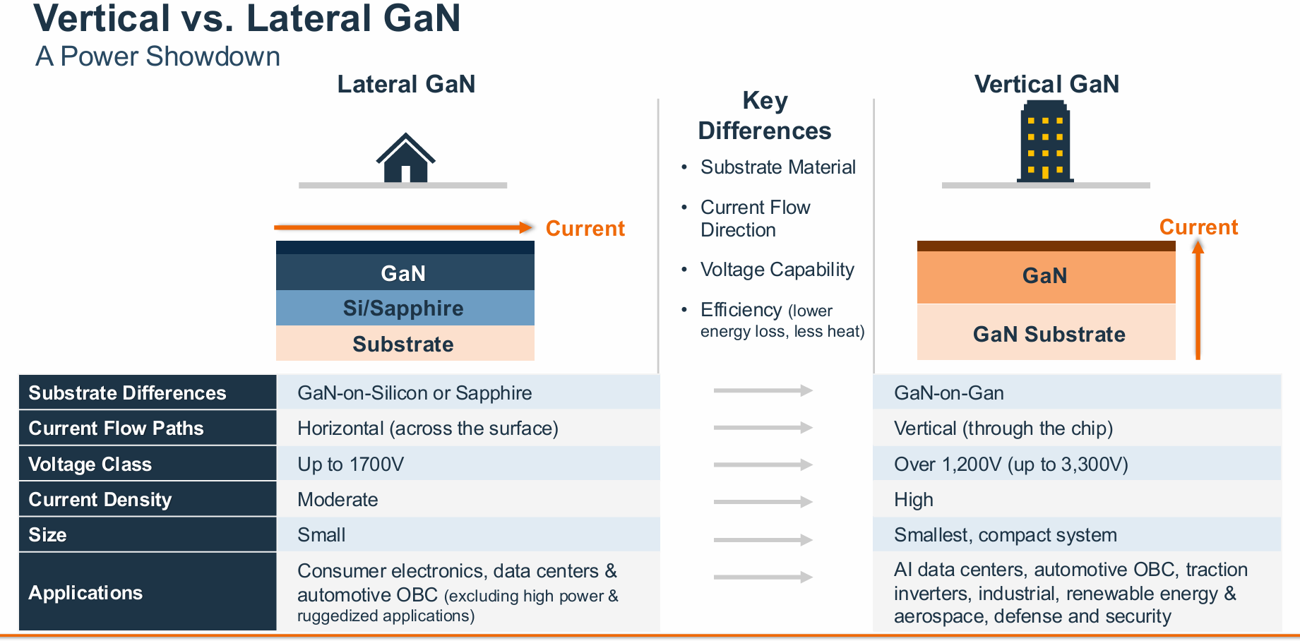
Lateral GaN vs vertical GaN. Source: onsemi
To help onsemi’s efforts in lateral GaN, the company and China’s Innoscience recently signed a memorandum of understanding in the GaN arena. As part of the deal, onsemi plans to develop a line of lateral GaN power devices.
“This announcement is about lateral GaN products starting with 40-200V. It is not related to onsemi’s vertical GaN technology, which is for much higher voltages (1200V) and higher current applications,” according to officials from onsemi. “This announcement is about onsemi securing lateral GaN wafer capacity with Innoscience, a leader in lateral GaN manufacturing. This is not an exclusive partnership.”
Meanwhile, this week, onsemi signed a separate agreement with GlobalFoundries (GF) to develop and manufacture GaN power products using GF’s 200mm GaN-on-silicon process, starting with 650V products.
As part of the plan, onsemi will pair its silicon drivers, controllers and packages with GF’s 650V GaN technology platform to deliver GaN devices with higher power density and efficiency. The proposed devices are targeted for power supplies and DC-DC converters. onsemi will begin sampling in the first half of 2026.
GF, the world’s fifth largest foundry vendor, has been expanding its efforts in GaN. In addition, the company recently licensed GaN technology from TSMC.
More GaN
Meanwhile, in recent times, there have been other major announcements in the GaN market, including:
*Ireland’s CHIPX plans to establish an 200mm GaN-on-SiC wafer fabrication facility in Malaysia, according to a report from Compound Semiconductor, a news site.
*Vertical Semiconductor, a Boston-based startup, recently emerged and introduced a new vertical GaN device technology.
*Israel’s VisIC Technologies, a supplier of GaN power semiconductors, announced the closing of its Round B funding, securing $26 million. The round was led by Hyundai Motor, Kia and others.
Then, at IEDM, several entities presented papers on GaN. Many of these efforts are still in the R&D stage. Here are some of the more novel papers:
*Dynax Semiconductor, Xiaomi Communications and the Hong Kong University of Science and Technology demonstrated a GaN power amp MMIC for mobile handsets. Researchers demonstrated a GaN-on-silicon low-voltage HEMT technology achieving a peak power added efficiency (PAE) of over 80%.
*Intel demonstrated a GaN chiplet technology based on a 300mm GaN-on-silicon process. “This GaN chiplet technology features: (a) the industry’s thinnest GaN chiplet with an underlying silicon substrate that is only 19µm thick, harvested from a fully-processed, thinned and singulated 300mm GaN-on-silicon wafer; (b) the industry’s first library of fully functional integrated on-die CMOS digital circuits, from inverters, logic gates, multiplexers, and flip-flops to ring oscillators, using monolithically integrated GaN N-MOSHEMT and a silicon PMOS process; (c) and promising results in TDDB, pBTI, HTRB and HCI studies indicating that the 300mm GaN MOSHEMT technology can meet the required reliability metrics,” according to a paper from Intel.
*KAIST reported the first demonstration of a heterogeneous 3D integrated RF platform that monolithically integrates indium gallium arsenide (InGaAs) and GaN HEMTs as a single RF block. Researchers stacked the RF block onto a CMOS wafer with die-to-wafer bonding technology. This work shows that compact and high-frequency operations can be realized in an integrated environment for next-generation RF systems.
*National Yang Ming Chiao Tung University, Realtek Semiconductor and Taiwan Semiconductor Research Institute proposed a normally-off electrostatic discharge (ESD) clamp circuit with zero transient leakage current, specifically designed for monolithic GaN-based integrated circuits fabricated using a GaN-on-silicon process. The proposed design minimizes circuit area by integrating the timing and voltage detection functions.
*Xidian University demonstrated a GaN-based monolithic integrated platform on a high-resistivity silicon substrate for RF and logic applications using an Au-free metal technology. (Au is the symbol for gold.) Applications include mixed-signal devices, RF analog and digital logic circuits.
*Xidian University and the Xi’an Electronic Engineering Research Institute (XEERI) reported the first experimental demonstration of a high-performance, high-voltage fast avalanche pulse device (APD) based on GaN. Researchers fabricated fast APDs on native GaN substrates, incorporating field plates and small-angle junction termination extensions.