


Options, Challenges For Wafer Bonding In Advanced Packaging
Executives from Kulicke & Soffa (K&S) sat down to talk about IC packaging, a new U.S. consortium, and the options for wafer bonding in advanced packaging.

By Mark LaPedus
Bob Chylak, senior vice president and chief technology officer of Central Engineering at Kulicke and Soffa (K&S), and John Molnar, vice president of advanced solutions at K&S, sat down with Semiecosystem to discuss Moore’s Law, IC packaging, a new U.S. consortium, and the options and challenges for wafer bonding in advanced packaging.
Semiecosystem: Can you briefly describe K&S and the company’s charter?
Chylak: K&S has a long history in the design, and production of assembly systems and solutions used throughout the semiconductor manufacturing process. Our innovations directly support high-volume semiconductor production, and new trends in diverse markets, such as consumer, automotive, power and battery, display, and advanced packaging.
Within semiconductor assembly, we are market share leaders in wire bonding for both ball and wedge bonders and wafer-level packaging assembly. Our assembly equipment supports the general growth of electronics used in smartphones, automobiles and computers, and the growing market of electronics everywhere. We have strong growth in high-performance computing applications for generative AI and machine learning markets with our thermo-compression bonding equipment, which has a lot of momentum. K&S is moving into new markets, including advanced dispense and display, which are growth vectors for the company.
Semiecosystem: Years ago, IC packaging was considered an afterthought in the semiconductor industry. An IC package was a relatively simple unit that basically encapsulated a chip. More recently, IC packaging, particularly advanced packaging, has become an important part of the semiconductor industry. Why? And what role does packaging play now?
Chylak: For almost 50 years, IC performance, power efficiency, form-factor and cost were provided by transistor shrinks following Moore’s Law. More transistors per wafer drove down wafer cost, and therefore IC cost, and improved performance, which led to higher profits and reinvestment.
The benefits of transistor shrinks began to diminish significantly in the mid-2010s, driven by higher design costs and yield challenges necessary to achieve higher density on wafers. Today, creating a fab node reduction costs more than the previous node. This breaks the cycle of performance improvements driving lower cost and investment, and has led to the end of Moore’s Law.
Today, 2D and 3D packaging has replaced transistor shrinks as the enabler for IC and package performance. So, assembly packaging via chiplet or heterogeneous integration has come to the forefront and has replaced fab node shrinks as the industry driver. K&S is positioned to take advantage of this by providing advanced assembly equipment and processes to support new assembly requirements.
Semiecosystem: Advanced packaging grabs most of the headlines these days. But it’s safe to say that a large percentage of today’s chips are housed in legacy and mature package types. Those mature IC packages won’t go away anytime soon. Plus, the semiconductor industry still relies on age-old wirebonding and flip-chip techniques. Any thoughts on these topics?
Chylak: Wire bonding, which includes both ball and wedge bonding and now vertical wire bonding, will continue to play a very central role in high-volume markets for a variety of reasons. First and foremost, it is the most cost-effective solution with a huge installed infrastructure, which allows for low capital expenditure.
Also, wire bonding is extremely flexible. You can stack dies with wire bonding in all types of various ways and lay out design modifications without major redesign efforts. Being the lowest cost solution, it is suitable and appropriate for more than 75% of ICs produced in the world, which will continue for the foreseeable future.
Semiecosystem: In the advanced packaging world, there is a lot of talk about chiplets. Chiplets are promising, but they are not a mainstream technology, at least right now. What are the challenges with chiplets and what’s holding them back?
Chylak: We continue to expect chiplets, or complex heterogeneous integration, to be increasingly essential to progressing performance, power efficiency, form-factor and cost targets for the industry. Chiplet technology essentially separates a microprocessor system, into module building blocks, and then connects these individual components into a larger working system, which is much more complex than a single die. There are many benefits to this approach: higher I/O density, lower cost as compared to a system-on-chip, shortened design cycle, and the ability to combine circuits from different technology nodes into one package, lowering overall cost.
Some of the challenges of developing these applications are design, verification, testing, and packaging. New EDA and design simulation tools, including thermal simulation are required. Higher complexity substrates with finer line-space specs are needed for these complex designs. Standards for die-to-die communication are needed. Testing capabilities present challenges as it is important to ensure the chiplets are functional before final packaging.
Recently we have begun to see greater traction with our assembly and test customers as well as foundry and IDM customers. We continue to see high-volume consumer, power and industrial applications moving more aggressively to develop innovative chiplet-based products, in addition to advanced logic.
Semiecosystem: 2.5D, one advanced package type, is taking off, thanks to AI. In 2.5D, you might have a GPU sitting next to a memory stack in the same package. The memory stack is called high-bandwidth memory (HBM). Both the GPU and HBM reside on an interposer. Today, the GPU is bonded to the interposer using a technique called solder-based thermal compression bonding (TCB). The individual DRAM dies in the HBM stack are also bonded together with traditional TCB. What bump pitches are we talking about here? Are there any challenges with solder-based TCB as the industry moves towards more advanced 2.5D packages and HBM?
Chylak: 2.5D is essentially a system-in-package that utilizes an interposer, which allows increased I/O density between chips. Today, these types of packages are only viable with pitches above 40µm with traditional solder-based TCB. Below this pitch, flux residue becomes very difficult to clean. Flux residue can lead to reliability failures for these expensive packages.
K&S has developed a Fluxless TCB process to overcome these issues. Despite the innovations in processing capability of these AI and high-performance computing applications recently, the interconnect density will continue to increase. Looking at the broad semiconductor market, including recent leading-edge chiplet-based packages, the vast majority of semiconductor applications are still well above 40µm pitches, but designs down to 10µm and below are already being tested. This creates lots of opportunities for our Fluxless TCB system, which extends down to sub-10µm pitches.
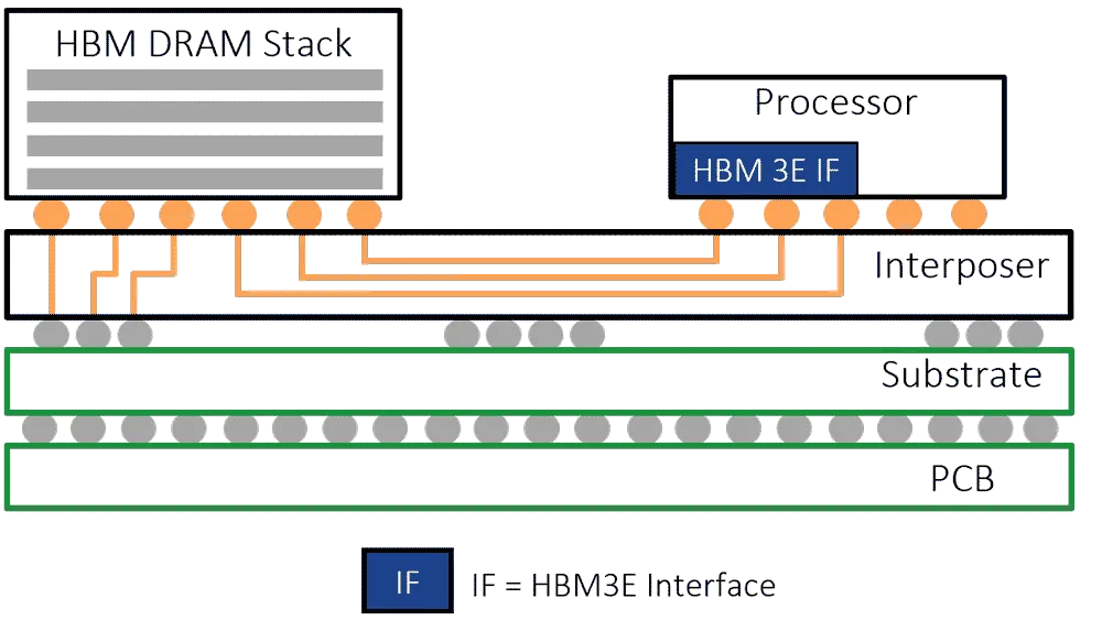
A typical 2.5D package. An HBM DRAM stack and a processor or GPU are situated on an interposer in the same package. HBM and the processor are electrically connected to each other. Source: Rambus
Semiecosystem: K&S has a Fluxless TCB tool. What is Fluxless TCB? What are the advantages of fluxless over traditional TCB? Does fluxless have a higher cost-of-ownership over traditional TCB?
Molnar: We are very proud of our innovations, as well as being first to volume production in Fluxless TCB. Through our partnerships and long-term development focus, we have developed TCB equipment that has removed the need to use flux. This enables a high-yielding interconnect process for tighter pitches between 40µm to about ~12µm.
TCB flux processes require a cleaning process to remove any residual flux. When the pitch becomes too tight, generally below 40µm, cleaning the flux becomes challenging and can result in short-term yield, or long-term reliability issues. Our Fluxless TCB systems are more complex than traditional TCB, requiring a higher ASP, but also provide an improved interconnect over a flux process, which customers have shown to improve overall yield.
Below 12µm, we have demonstrated the ability to remove the solder and go with a direct copper-copper interface. We call this a ‘CuFirst’ hybrid process. There are huge advantages for this CuFirst hybrid process over a standard hybrid process. It is much lower cost, does not require a class 1 cleanroom environment, and the same equipment that runs a 40µm solder interconnect process can be used for the CuFirst process at finer pitches. We believe this solution is a lower cost, higher yield solution compared to hybrid, and can work down to ~3µm pitch and potentially below. While we anticipate traditional TCB applications to ultimately transition to Fluxless TCB applications, Fluxless TCB is also increasingly becoming an alternative to hybrid bonding.
Semiecosystem: What are the main applications for Fluxless TCB? How far does it extend? Will it go beyond sub-10µm pitches?
Molnar: Advanced logic transitions to 3D and 2.5D applications are a major focus, although as the pitch decreases below 30µm, the market will broaden to more cost-sensitive applications utilized in consumer, automotive, and industrial-related projects, driving increased capacity requirements for Fluxless TCB. We are confident in moving to sub-10µm pitches and have recently began working on a specific sub-10µm application with a major customer. Beyond Fluxless TCB, CuFirst can provide even a tighter pitch performance.
Semiecosystem: Beyond a certain pitch, you need hybrid bonding for wafer-to-wafer and die-to-wafer bonding. Isn’t hybrid bonding being used today for CMOS image sensors and some advanced packaging work? What are the advantages of using hybrid bonding?
Chylak: Hybrid bonding on a wafer-to-wafer process has been in high-volume production for several years at this point. The primary application for wafer-to-wafer hybrid was primarily for devices like CMOS image sensors, which require an optical component and a logic component. When both the optical wafer and logic wafer have high yields and are designed to be integrated together, hybrid bonding can be deployed at the wafer level.
For chiplets, which include more complex architectures than the two identically sized chips of the CMOS example, a die-to-wafer hybrid, or die-to-wafer TCB as opposed to wafer-to-wafer, are required, which utilize known good die and provide more assembly flexibility. Hybrid bonding advantages are that it can be completed largely in a room temperature environment, can extend the pitch beyond 10µm and can reduce the vertical height of the interconnect since it is a bumpless process.
The challenges with hybrid are the requirements for additional front-end processing steps, fab-like clean-room environments and poorer yields than TCB. We estimate hybrid is multiple times the production cost of TCB, which limits it to applications that can withstand very high prices. K&S has developed a CuFirst hybrid bonding process that can be assembled on our Fluxless TCB machine in a normal assembly factory. Our first customer in production will be announced before the end of the year.
Semiecosystem: What are the challenges with hybrid bonding in general?
Molnar: Yield and expense. It is a very elegant process, although it requires a much cleaner environment than other back-end processes, which has restricted broader adoption. The potential customer base is really limited to sizeable foundry and IDM customers willing to deploy front-end capacity. Additionally, we do not anticipate significant end applications that require the pitch density hybrid offers beyond Fluxless TCB.
Semiecosystem: K&S has a product called APTURA. Can you describe it? How does it work?
Molnar: APTURA is our latest TCB platform that is fluxless and direct copper-to-copper capable. This system can be configured with a chip-to-chip or chip-to-wafer configuration and is capable of sourcing chips from reel, tray or directly from a wafer and placing them on substrates, interposers, wafers, or other chips.
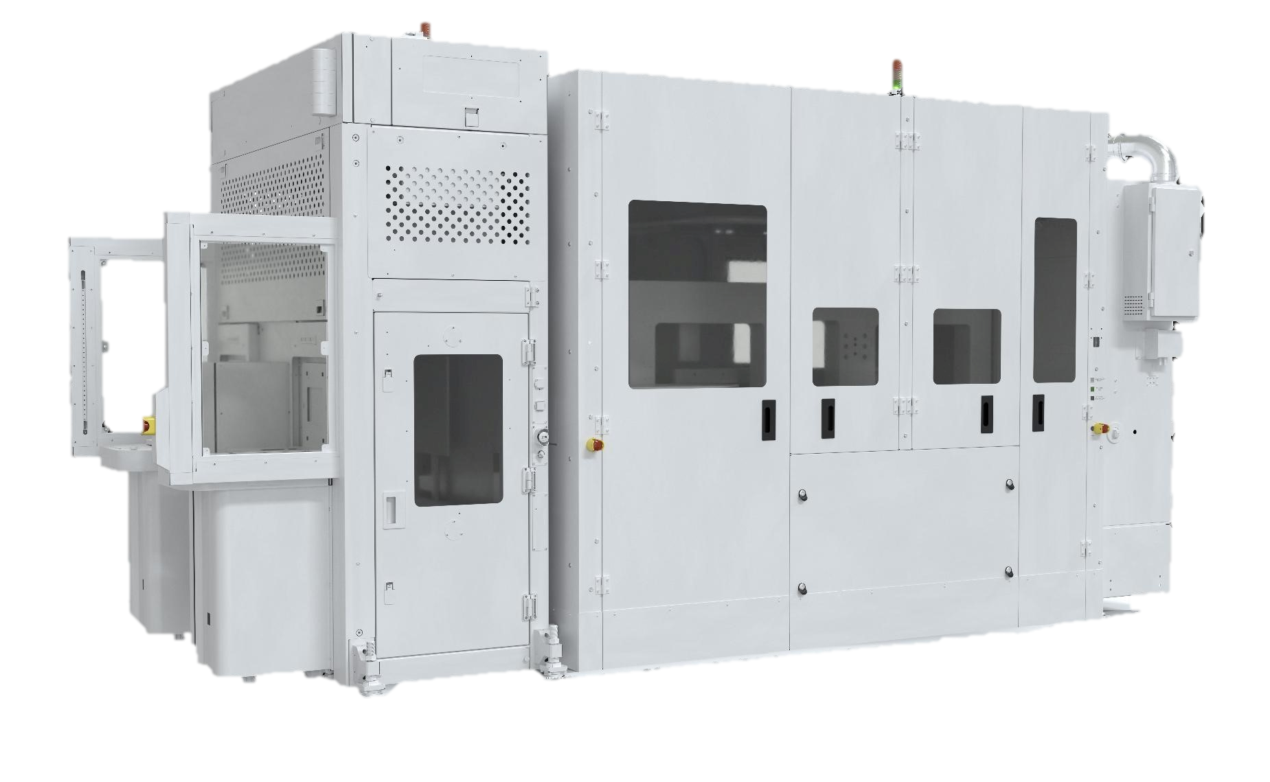
K&S’ APTURA platform Source: Company
Semiecosystem: Is it safe to say that no one bonding technique will rule the advanced packaging world? TCB will be used for some applications, while hybrid bonding will be used for others, right?
Chylak: We agree many advanced packages, such as system-in-package, 2.5D or 3D, will include several different interconnect technologies. We clearly expect a significant increase in Fluxless TCB in high-end logic markets, growth of different materials and module-based packages in power semiconductor, and more wire bonding, as well as TCB in high-volume markets. We also have plans to extend our CuFirst hybrid down to 3µm pitch and below.
Semiecosystem: Resonac and others recently launched a new packaging consortium called US-JOINT. The consortium also includes Azimuth, KLA, K&S, Moses Lake Industries, MEC, ULVAC, NAMICS, TOK and TOWA. What is this consortium all about? What is the charter?
Chylak: Advanced packaging has been discussed for years, with market adoption primed to accelerate. This recent consortium is the third global ‘Joint’ consortium led by Resonac – a major supplier of materials used across the semiconductor industry – and the first one in the U.S. This consists of membership of five Japanese and five U.S.-based companies with a broad charter to accelerate the development of advanced packaging technologies. This facility will allow IC design companies without assembly competencies and capacity to validate their package designs instead of relying on existing subcontractors or wafer foundries. This collaboration also allows the consortium members to better understand the needs and direction of future advanced applications.
While semiconductor assembly production has largely shifted to Asia over the past 20 years, semiconductor design has actually increased in the U.S. With packaging technologies being critical to continuing the spirit of Moore’s Law, bringing advanced packaging capabilities back to Silicon Valley, is a necessary step that we are happy to be part of. We expect this Union City, Calif.-based facility to fully operational by the end of 2025.