
PackageEcosystem Report: Nvidia, Micron, Ayar, HBM
This (free) report provides a snapshot of the latest announcements in packaging and other markets

By Mark LaPedus
IC packaging is an important part of the semiconductor industry. Packaging is also a complex business with a multitude of facets. Plus, there is frenetic wave of new announcements in packaging. It’s hard to keep up with the announcements.
Test is also important. To help the industry, Semiecosystem has released its first edition of “The PackageEcosystem Report.” This report provides a snapshot of the latest announcements in packaging and other markets. (The report is free for readers.) Here’s what this report covers:
1—Nvidia’s $4B deals
2—Micron expands
3—Ayar Labs obtains funding
4—HBM vs HBF vs ZAM
5—New 3DIC contender?
6—HBM4E memory controller
7—Broadcom’s 3.5D packaging
8—CIH’s RF modules
9—Glass fiber for packaging
10—Imec’s PDKs for advanced packaging
Nvidia’s $4B deals
Nvidia, the leading supplier of AI chips, has announced separate and major agreements with two companies--Coherent and Lumentum Holdings.
As part of these major announcements, Nvidia has invested a total of $4 billion in Coherent and Lumentum. The funding will be used to help Nvidia obtain the necessary components for its new co-packaged optics (CPO) technology. Basically, CPO is a packaging technology that boosts the performance of systems in AI datacenters.
In the first deal, Nvidia and Coherent announced a multiyear strategic agreement to advance the frontier of advanced optics technologies, including manufacturing capacity and research and development, to enable next-generation AI infrastructure.
The nonexclusive agreement includes an Nvidia multibillion-dollar purchase commitment and future access and capacity rights for advanced laser and optical networking products. In addition, Nvidia is investing $2 billion in Coherent to support research and development, future capacity and operations as Coherent builds out its U.S.-based manufacturing capabilities.
In the second deal, Nvidia announced multiyear strategic agreements with Lumentum Holdings to accelerate innovation in advanced optics technologies, including research and development, to enable next-generation AI infrastructure and systems designs.
The nonexclusive agreement includes an Nvidia multibillion purchase commitment and future capacity access rights for advanced laser components. In addition, Nvidia is investing $2 billion in Lumentum to support R&D, future capacity and operations as the company builds out its U.S.-based manufacturing capabilities in a new fab.
Micron expands
For some time, there has been an acute shortage of DRAMs, high bandwidth memory (HBM) and NAND flash memory products in the global market. Memory prices are also skyrocketing.
Suppliers of memory products are scrambling to meet demand. And many memory vendors are expanding their manufacturing capacities to meet demand.
For example, U.S.-based Micron Technology is expanding both its fab and packaging capacity. This week, Micron moved into production in its new semiconductor assembly and test facility in Sanand, Gujarat, India.
This facility represents a combined investment of approximately $2.75 billion by Micron and its government partners, advancing semiconductor manufacturing capabilities in India. Other companies are also building packaging facilities and fabs in India.
Once fully ramped, the first phase of Micron’s Sanand operation will feature more than 500,000 square feet of cleanroom space. Micron’s facility converts advanced DRAM and NAND wafers from the company’s manufacturing network into finished memory and storage products. The site serves customers worldwide to meet the growing global demand for memory and storage.
To mark the grand opening of the site, Micron presented its first shipment of made-in-India memory modules to Dell Technologies for its laptops made in India for India. The Sanand site is ISO 9001:2015 certified. Micron expects to assemble and test tens of millions of chips at Sanand in 2026, scaling to hundreds of millions in 2027.
In recent times, Micron has also been expanding its fab capacity. Here’s the company’s latest announcements:
*In January 2026, Micron broke ground on its $100 billion leading-edge memory manufacturing complex in Onondaga County, New York. With up to four fabs, this will be the largest semiconductor facility in the United States, generating 50,000 jobs in New York. Production is expected to start in 2030 with the fabs ramping throughout the decade.
The New York project is a cornerstone of Micron’s approximately $200 billion broader U.S. expansion vision, which also includes two leading-edge high-volume fabs in Idaho, the expansion and modernization of its existing manufacturing fab in Virginia, and advanced HBM packaging capabilities.
*In January 2026, Micron signed an exclusive Letter of Intent (LOI) to acquire Powerchip Semiconductor Manufacturing Corp.’s (PSMC) P5 fabrication site in Tongluo, Miaoli County, Taiwan, for total cash consideration of US$1.8 billion. The acquisition includes an existing 300mm fab cleanroom of 300,000 square feet. The LOI also aims to establish a long-term relationship between Micron and PSMC for Micron’s post-wafer assembly processing and to support PSMC in its legacy DRAM portfolio.
*In January 2026, Micron broke ground on an advanced wafer fabrication facility located within the company’s existing NAND manufacturing complex in Singapore. This new facility represents a planned investment of approximately US$24 billion (SG$31 billion) over 10 years and is designed to ultimately provide 700,000 square feet of cleanroom space. Wafer output is scheduled to begin in the second half of calendar 2028.
Ayar obtains funding
Ayar Labs, a supplier of co-packaged optics (CPO) solutions for AI, announced the closing of $500 million in Series E funding led by Neuberger Berman.
Neuberger Berman will take a board observer role at Ayer. Based in San Jose, Calif., Ayer will use the funds to scale high-volume production and test capacity to accelerate the deployment of its CPO solutions. This brings the company’s total funding to $870 million and raises the company’s valuation to $3.75 billion.
New investors include Alchip Technologies, ARK Invest, Insight Partners, MediaTek, Qatar Investment Authority (QIA), Sequoia Global Equities, and 1789 Capital. They join existing financial institutions such as Advent Global Opportunities, Boardman Bay Capital Management, IAG Capital Partners, Light Street Capital, and Playground Global, and existing strategic investors, AMD Ventures, and Nvidia.
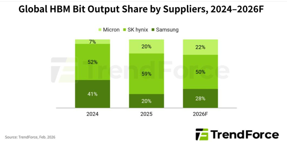
HBM vs HBF vs ZAM
High bandwidth memory (HBM) is the key memory technology for AI chip architectures.
In recent times, several companies have introduced two new and potentially competitive technologies to HBM--High Bandwidth Flash (HBF) and Z-Angle Memory (ZAM).
South Korea’s SK hynix and U.S.-based Sandisk are pushing HBF. Both companies have started the standardization process for HBF.
HBF resembles HBM. But in HBF, you vertically stack NAND dies on an interposer. HBF technology can fill the gap between HBM and SSDs. While HBM handles high-level bandwidth, HBF technology serves as a supporting layer in the architecture.
“The first-generation product delivers blazing-fast read bandwidth of 1.6 TB/s and packs 256Gb per die, reaching 512GB total capacity per 16 die stack while closely matching the physical footprint, power profile, and stack height of HBM4,” according to Sandisk. “HBF is purpose-built to meet the scale and intensity of next-generation AI inference workloads, offering the performance needed without compromising on capacity or efficiency.”
SK hynix and Sandisk are pursuing HBF standardization and commercialization based on their design, packaging and mass production experience in HBM and NAND.
Meanwhile, SoftBank’s subsidiary, SAIMEMORY, recently signed a collaborative agreement with Intel. The companies plan to commercialize ZAM, a next-generation memory technology designed for high capacity, high bandwidth and low power consumption.
The goal is to produce prototypes in fiscal year ending March 31, 2028, and achieving commercialization in FY2029, according to U.S.-based Intel and Japan’s SAIMEMORY. Click here for a description of ZAM from Semivision.
The question is clear here: Does the industry need another high-end memory architecture? Both HBF and ZAM are promising, but it’s unclear why the industry needs these products. Both look like niche products, that is, if they ever move from the lab to the fab.
For now, HBM will dominate the landscape. Now, suppliers of HBM are racing each other to ship next-generation HBM4 products.
Nvidia’s upcoming Rubin platform is expected to become a major catalyst for HBM4 adoption once mass production begins, according to TrendForce, a research firm. “The three leading memory suppliers—Samsung, SK hynix, and Micron—are now in the final stages of HBM4 validation, with completion anticipated by 2Q26,” according to TrendForce. “Samsung, supported by its strong product stability, is projected to secure certification first. SK hynix and Micron are expected to follow shortly thereafter, forming a three-supplier ecosystem for Nvidia’s HBM4.”
New 3DIC contender?
Is there another contender in the 3D mix?
Belgium’s Vertical Compute, a spinoff of Imec, has raised €57 million (US$66 million) in funding. Quantonation led the seed round, with participation from Flanders Future Techfund, Wallonie Entreprendre, Sambrinvest, Noshaq, InvestBW, Drysdale Ventures and Kima Ventures. Existing investors, Eurazeo, XAnge, Vector Gestion, imec.xpand and Imec, also reinvested in this round.
Vertical Compute is developing a new technology. It plans to integrate memory directly above compute logic within a single wafer manufacturing process, reducing data movement from centimeters to nanometers.
Rather than replacing compute cores, Vertical Compute is developing an enabling layer—enhancing CPUs, GPUs and custom AI accelerators with higher memory density and bandwidth.
In just over a year, Vertical Compute has taped-out the company’s first test chip, integrating vertical memory stacks directly on compute logic within a single 300mm wafer manufacturing process flow.
HBM4E memory controller
Rambus has rolled out an HBM4E Memory Controller IP product line. The HBM4E Controller enables a new generation of HBM memory deployments for cutting-edge AI accelerators, graphics and HPC applications.
The HBM4E Controller is capable of supporting operation up to 16 Gigabits per second (Gbps) per pin, providing a throughput of 4.1 Terabytes per second (TB/s) to each memory device. For an AI accelerator with eight attached HBM4E devices, this translates to over 32 TB/s of memory bandwidth for next-generation AI workloads. The HBM4E Controller IP can be paired with third-party standard or TSV PHY solutions to create a complete HBM4E memory subsystem in a 2.5D or 3D package as part of an AI SoC or custom base die solution.
3.5D packaging
Broadcom has begun shipping a 2nm custom compute system-on-a-chip (SoC) built on its 3.5D eXtreme Dimension System in Package (XDSiP) platform.
Broadcom has shipped its first 3.5D custom compute SoC to Fujitsu. 3.5D XDSiP combines 2.5D techniques and 3D-IC integration using face-to-face (F2F) technology, according to Palo Alto, Calif.-based Broadcom.
With 3.5D XDSiP, AI chip customers can deliver XPUs with signal density, power efficiency and low latency to meet the massive computational demands of gigawatt-scale AI clusters. Here are the key benefits for Broadcom’s 3.5D XDSiP:
*Interconnect Density – “Achieves a 7x increase in signal density between stacked dies compared to F2B technology,” according to Broadcom.
*Power Efficiency – “Delivers a 10x reduction in power consumption in die-to-die interfaces by utilizing 3D HCB instead of planar die-to-die PHYs,” according to Broadcom.
*Reduced Latency – “Minimizes latency between compute, memory, and I/O components within the 3D stack,” according to Broadcom.
*Compact Form Factor – “Enables smaller interposer and package sizes, resulting in cost savings and improved package warpage,” according to Broadcom.
RF modules
Circuits Integrated Hellas (CIH) has rolled out the CI-ONE family of small-form-factor integrated PA + SPDT modules.
The module combines a power amplifier (PA) and RF switch (SPDT) in the same unit. Positioned among the industry’s most advanced integrated PA + SPDT solutions for Ka-band applications, CI-ONE delivers ultra-fast (5ns) switching speeds for next-generation Satcom architectures vital in 5G/6G, radar and aerospace applications, according to CIH. Headquartered in Athens, Greece, CIH is a supplier of RF chips and other products.
Conventional switched Ka-band transmit front-ends rely on discrete power amplifiers and RF switches, increasing PCB area, system cost, thermal complexity and design effort. CI-ONE collapses these functions into a single, compact, surface-mount module—integrating a high-performance power amplifier and SPDT switch in one optimized device.
As a result, the modules are approximately 3X smaller, up to 50% less costly, and up to 20% more efficient than conventional discrete PA + SPDT implementations.
Fabricated using a GaAs pHEMT process, the CI-ONE family operates from a 6V supply and supports three output power classes—30 dBm, 34 dBm and 36 dBm variants—enabling design flexibility across 1W, 2W, and 4W system requirements. With fast switching performance of 5ns and efficiency of approximately 22% at the 1 dB compression point (P1dB), CI-ONE enables transmit architectures without sacrificing power-added efficiency.
The CI-ONE family of integrated Ka-band switch power amplifiers will be available in Q4 2026, with early engagement and sampling programs beginning prior to general release.
In a separate move, CIH and Reach Power announced a memorandum of understanding (MOU) establishing a multi-year strategic alliance between the two companies. Focused on joint development of integrated radio frequency (RF)/millimeter-wave (mmWave) and wireless power and data transfer (WPDT) solutions, the alliance will target Satcom, defense, energy transfer, and other phased-array applications.
Under the MOU, CIH will serve as a semiconductor design partner and chip supplier, including RF/mmWave ICs, system-level beamforming architectures, and heterogeneous integration approaches tailored for high-performance satellite and networked power systems.
Based in Redwood City, Calif., Reach Power will contribute its wireless power-at-a-distance technology, AI-optimized power-beaming control algorithms, and system integration expertise across platforms that demand simultaneous power and data delivery.
Glass fiber deal
AGY has announced a strategic partnership with JPS Composite Materials. The companies plan to manufacture and produce the first North American-based low coefficient of thermal expansion glass fiber fabric designed specifically for advanced integrated circuit (IC) substrates and next-generation semiconductor packaging technologies.
Based in Aiken, S.C., AGY is a manufacturer of advanced specialty glass fibers. Based in Anderson, S.C., JPS leads the way in the manufacturing of high strength fiberglass, quartz, para-aramid, and specialty composite reinforcement fabrics.
Together, the companies are establishing a fully domestic supply chain for critical reinforcement materials used in high-performance semiconductor applications. Low CTE glass fiber fabric plays a vital role in IC substrate performance by enhancing dimensional stability, reducing warpage, and supporting higher interconnect density. These characteristics are essential for advanced packaging platforms such as Chip-on-Wafer-on-Substrate (CoWoS) and System-on-Integrated-Chips (SoIC), which enable higher bandwidth, improved power efficiency, and greater functional integration in AI, data center, and high-performance computing applications.
Imec releases PDKs for advanced packaging
Belgium’s Imec recently inaugurated its NanoIC pilot line. The pilot line specifically targets the development of beyond-2nm systems-on-chip (SoC) designs.
The NanoIC pilot line has released two advanced interconnect process design kits (PDKs): a fine-pitch redistribution layer (RDL) and die-to-wafer (D2W) hybrid bonding PDK.
These PDKs, built on the NanoIC pilot line, give designers early access to the design rules and validated building blocks needed to explore high‑density chip‑to‑chip integration. These early-access PDKs bring advanced packaging capabilities within reach of universities, startups, and industry innovators.