
Scaling Copper Interconnects To 2nm And Beyond
Applied Materials has developed a copper interconnect process for advanced chips at 2nm and beyond

By Mark LaPedus
At the recent Symposium on VLSI Technology and Circuits in Japan, Applied Materials presented a paper that describes a way to extend copper interconnects for advanced logic chips at the 2nm process node and beyond.
Applied has developed a copper interconnect process flow, which utilizes various equipment and materials, including a new low-k dielectrics line and a ruthenium-cobalt (RuCo) liner technology. In the paper, Applied demonstrated the viability of this process by developing an AI accelerator test chip, based on the latest transistor technology at the 2nm node.
To be sure, this is a complex process with several facets. In simple terms, an advanced logic chip incorporates billions of tiny structures called transistors. A transistor, which is a key building block in chips, is used to switch the electrical signals in the device.
In the same advanced chip, the tiny transistors are electrically connected to each other using a complex copper wiring scheme. This wiring scheme, called the copper interconnects, is an important part of the chip.
But in recent times, chipmakers have encountered several challenges and issues with the copper interconnects. Basically, the tiny wires in the copper interconnects have become smaller and more compact at each node, thereby potentially creating electrical resistance and other problems in this complex wiring scheme. This impacts the performance and reliability of a chip.
The challenges are expected to escalate at the 2nm process node and beyond. Looking to solve these and other issues, Applied’s new process paves the way towards the development of these complex copper interconnects for advanced chips at the 2nm node and beyond. “There is an urgent need for process innovations, which enable resistance and capacitance reduction without compromising reliability and yield,” said Gaurav Thareja, director of logic and memory process integration at Applied, in the paper. Others contributed to the work.
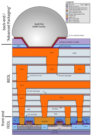
Transistor with copper interconnects. The transistor is located on the bottom of the structure (FEOL). Copper interconnects (orange color) are formed on top of the transistor (BEOL). There are several levels of copper interconnects. Source: Wikipedia
The basics
Nearly every system, such as appliances, cars, computers, game machines, GPS units, medical equipment, TVs, smartphones and other products, are powered by chips. Many systems incorporate a multitude of chips. A car, for example, incorporates from 1,000 to 3,000 different chips.
Basically, a semiconductor, or chip, incorporates complex electronic circuitry, allowing a chip to perform a specific function in a system. Chips are manufactured in giant facilities called fabs.
The semiconductor industry produces a plethora of different chip types. For example, a processor is used to power PCs and smartphones. GPUs are chips that drive the graphics in game machines, PCs and phones. GPUs are also used to accelerate AI algorithms in computers. Memory chips store data. There are many other chip types as well.
Generally, an advanced logic chip incorporates several key pieces or components, including transistors, interconnects and contacts. A transistor is used to amplify or switch electrical signals in chips. Chipmakers (i.e. Intel, Samsung, TSMC, etc.) manufacture the transistors and other components in one part of the fab, which is called the front-end-of-line (FEOL).
Each advanced chip consists of billions of tiny transistors. You need to electrically connect the transistors in the chip. Otherwise, the chip may not work properly or could fail in a system.
To connect the transistors, a chipmaker will fabricate a complex copper wiring scheme above the transistors. This wiring scheme, called the copper interconnects, electrically connects the transistors in the chip. A chip may have several levels of copper interconnects.
In operation, the interconnects distribute the power and route electrical signals in the chip. The copper interconnects are manufactured in another part of the fab called the back-end-of-line (BEOL).
Then, in the fab, chipmakers also manufacture a middle-of-line (MOL) layer. This layer consists of a multitude of tiny contact structures, which electrically connect the separate transistor and copper interconnect structures. And if that’s not enough, future advanced chips may also incorporate a backside power delivery network module. This module will route the power lines in the backside of the chip.
Early transistors and interconnects
To get a handle on what’s next in semiconductor technology, it’s a good idea to look back and examine the evolution of transistors and interconnects. The modern semiconductor industry can be traced back to 1947, when Bell Labs invented the transistor. Then, in the 1958 and 1959 timeframe, Texas Instruments and Fairchild Semiconductor co-invented the integrated circuit (IC). An IC incorporates transistors and other components on the same chip.
In 1959, Fairchild’s Jean Hoerni invented the planar process, which “improved transistor reliability by creating a flat surface structure protected with an insulating silicon dioxide layer,” according to the Computer History Museum. Building on this invention, Fairchild’s Robert Noyce devised a way to connect the transistors and other components using aluminum interconnects on top of the device. Thus, Noyce invented the monolithic IC. (Noyce also co-founded Intel in 1968.)
Meanwhile, starting in the 1960s, the metal–oxide–semiconductor field-effect transistor (MOSFET) emerged as a common transistor type in digital circuits. Aluminum interconnects were also used in early devices.
The MOSFET is still used in many of today’s chips. A MOSFET is a planar structure, which consists of source, gate and drain. “The area between the source and drain is called the ‘channel,’ controlled by a ‘gate’ on top,” according to Intel. “When the gate is off, current can’t flow from the source to the drain. The gate is turned on by applying a voltage to the gate to attract the appropriate charge in the channel. This completes the connection between source and drain, allowing current to flow.”
Transistors can be combined to form logic gates. Logic gates are combined, creating more complex circuits.
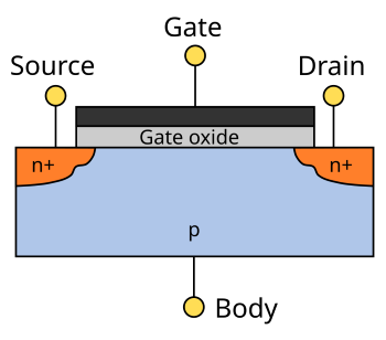
MOSFET Source: Wikipedia
Aluminum to copper interconnects
Fast forward. In 1981, IBM introduced the 5150 Personal Computer, a system that revolutionized desktop computing. This system wasn’t the world’s first PC. But IBM developed a system with an open architecture, enabling companies to develop IBM-compatible PCs or clones.
IBM’s PC was powered by Intel’s 8088 microprocessor, which was introduced in 1979. Manufactured using a 3μm process, Intel’s x86-based 8088 processor consisted of 29,000 transistors. In those days, aluminum interconnects were used in chips.
Intel’s 8088 wasn’t the company’s first microprocessor, but this chip gave rise to the x86-based architecture for the fledging PC industry. And in some respects, the processor also fueled what became the transistor scaling race in the semiconductor industry.
Several years earlier, Intel co-founder Gordon Moore published his famous paper, predicting that the number of transistors on an IC would double every year. In 1975, Moore revised this to doubling every two years.
This observation, called Moore’s Law, became a guiding principle for the semiconductor industry. Following this concept, Intel and other chipmakers in the 1970s began to race each other to introduce a new and more advanced manufacturing process every 24 or so months. A manufacturing process involves the steps and recipes to make chips in a fab.
Eventually, at each new process node, the goal among chipmakers was (and still is) to shrink, or scale, the select feature sizes of a transistor by 0.7x. By making the transistors smaller, you could cram more transistors on the same chip. Chipmakers also scaled the interconnects. This in turn enabled new and faster chips with more functions at each turn.
Thanks to transistor/interconnect scaling, Intel developed new and faster x86-based microprocessors at each new process node. This enabled new and faster PCs at lower price points. Thus, the PC market skyrocketed. Other chip markets also followed the same scaling concepts.
By the mid-1990s, though, the semiconductor industry hit a roadblock. Transistor scaling was alive and well, but aluminum-based interconnects were approaching their limits. In response, IBM developed a new solution: copper-based interconnects. Copper wires conduct electricity with 40% less resistance than aluminum, which resulted in a 15% boost in microprocessor speed, according to IBM.
In 1998, IBM introduced the PowerPC 740/750 microprocessor. Based on a 0.20μm process, the microprocessor incorporated 6.35 million transistors with the industry’s first copper interconnects.
At the time, IBM also developed a new manufacturing process, enabling copper interconnects in chips. That technology, called the dual-damascene process, became the standard way to develop copper interconnects in chips. The dual-damascene process is still used today.
The dual-damascene process takes place in the BEOL part of a fab. The goal is to develop several levels of copper interconnects on top of the transistors. In the first step of this process, a chipmaker deposits a dielectric material on the first layer of the interconnect structure. Then, the chipmaker will form trenches and vias in the dielectric materials using etch equipment.
Following that step, a chipmaker will deposit a thin barrier material on the sidewalls of the vias and trenches. Then, a liner material is deposited on the barrier material. Initially, the thin barrier layer consisted of a tantalum nitride (TaN) material, while liner used a tantalum (Ta) material.
Then, a copper material is deposited in the trench and vias. The barrier/liner materials prevent copper from diffusing into the dielectric materials.
This process is repeated several times. Thus, the chip consists of several levels of copper interconnects. The interconnects connect one level to another. And, of course, the interconnects are electrically connected to the transistors.
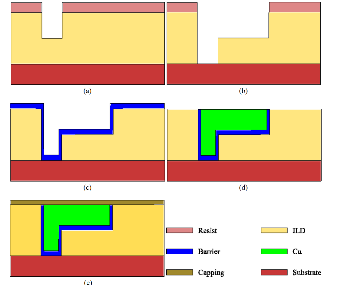
Copper dual-damascene fabrication process. (a) Via patterning. (b) Via and trench patterning. (c) Barrier layer deposition and Cu seed deposition. (d) Cu electroplating and excess removal by chemical mechanical polishing. (e) Capping layer deposition. Source: R. L. de Orio "Electromigration Modeling and Simulation" Dissertation, Institute for Microelectronics, TU Wien.
Planar transistors to finFETs and cobalt
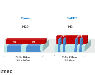
Up until 2010s, chipmakers continued to scale the transistor, along with the copper interconnects, enabling new chips. In the 2010s, though, the planar transistor reached its physical limits at the 20nm process node. A 20nm process consists of a 90nm contacted gate pitch (CPP), according to WikiChip, a technology site. CPP is the horizontal distance between the centers of two adjacent gate contacts.
Planar transistors are still used for chips at the 20nm node and above (i.e. 28nm, 40nm, 65nm, etc.). But at that time, the industry required a new transistor type for high-performance chips beyond 20nm.
In 2011, Intel introduced a new transistor type called the finFET at the 22nm node. Later, GlobalFoundries, Samsung and TSMC migrated to finFETs at the 16nm/14nm nodes. Unlike planar transistors, which are 2D structures, the finFET is a 3D-like device. FinFETs enable faster chips at lower power.
Planar vs finFET transistor Source: Imec
While the finFET solved one major problem, chipmakers faced another challenge at the 20nm node—the copper interconnects were becoming the speed bottleneck in chips. At that time, a leading-edge chip consisted of 9 to 13 layers of copper interconnects. At each node, the width of the copper wires became narrower. The interconnects also became more complex and compact.
Thus, there were (and still are) several challenges with the tiny copper interconnects, including the so-called resistance-capacitance (RC) delay. Basically, the RC delay causes a speed degradation in chips.
“The electrical resistance (R) of a material describes how difficult it is to move electrical current through a particular cross-section of that material,” according to Lam Research in a blog. “On the ‘C’ side, capacitance is a function of the insulating dielectric material around the metal lines and the distance between them. Higher capacitance slows electrons and can create unwanted cross talk.”
Fortunately, there was a solution here. At the 16nm/14nm process node in 2013 or so, chipmakers continued to utilize copper interconnects using the dual-damascene process.
But in general, chipmakers moved from tantalum (Ta) to a cobalt (Co) material for the liner in copper interconnects. Tantalum nitride (TaN) was still used for the barrier. That solution worked. Cobalt is a low resistivity material. It also adheres well to copper. A cobalt liner can increase the gap fill window of copper in narrow interconnects.
FinFETs, along with new materials in the copper interconnects, enabled the industry to develop advanced chips down to the 3nm node. For example, Apple’s latest iPhone chip is a 3nm device with 20 billion transistors. Generally, the 3nm node consists of a 48nm CPP.
Those innovations didn’t solve everything. In recent times, it has become more challenging and expensive to manufacture chips at the latest nodes. Plus, the price/performance benefits are diminishing at each node.
FinFETs to GAA with RuCo
Nonetheless, the workhorse finFET transistor will run out of steam beyond the 3nm node. So starting at the 2nm node in the second half of 2025, Intel and TSMC are expected to ramp up chips based on a new transistor type called gate-all-around (GAA). Some call it the nanosheet or ribbon FET.
In 2022, Samsung began shipping chips based on nanosheets at the 3nm node. Samsung is also developing a 2nm nanosheet technology.
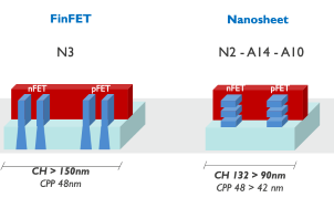
FinFET vs gate-all-around transistor Source: Imec
Nanosheets provide better performance than finFETs, but they are also harder and more expensive to make in the fab. In addition, there are some new challenges with the interconnects at the 2nm node and beyond.
Advanced logic chips can incorporate billions of transistors with over 18 metal layers. The width of the smallest wires is roughly 13nm. In total, a leading-edge chip may have 60 miles or more of copper interconnect wiring, according to Applied.
As the industry scales to 2nm and below, the dielectric materials become thinner. Thus, the chip becomes mechanically weaker. Plus, the RC delay issues aren’t going away.
To solve the problem, Applied has developed a BEOL interconnect process for the 2nm node and beyond. In Applied’s process, copper is still the conducting material. It still makes use of the dual-damascene process. “We see demand for new technologies to extend dual damascene for the foreseeable future,” Applied’s Thareja said.
But at the 2nm node and beyond, the copper interconnect process requires new equipment and materials. In some cases, for example, a binary metal combination of ruthenium and cobalt (RuCo) will be used for the liner material. Tantalum nitride (TaN) is still used for the barrier.
“TaN barrier layers continue to extend in large part due to breakthrough technologies,” Thareja said. “(For the liner), cobalt is still in use today at the most advanced nodes. For the smallest wires, both cobalt and RuCo are used, depending on the metal layer. RuCo has been adopted by all leading logic chipmakers for the 2nm node.”
A ruthenium-cobalt (RuCo) material reduces liner thickness by 33% to 20 angstroms. RuCo also produces better surface properties for void-free copper reflow. And RuCo reduces the resistance by up to 25%, thereby improving chip performance and power consumption, according to Applied.
In a 2nm test chip, Applied’s process, along with the RuCo liner and new low-k dielectrics, delivered a 2.5% performance boost over a standard process flow. A 2.5% boost doesn’t sound like much, but it adds up over time.
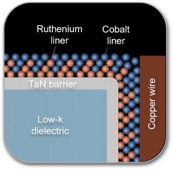
Copper interconnects with a RuCo liner and TaN barrier. Source: Applied Materials
Here's how Applied’s copper interconnect process flow works:
1-Dielectric deposition
In the fab, the chips are manufactured on a 300mm wafer in the fab. Then, it’s time to form the copper interconnects on top of the chips. The first step is to deposit a low-k dielectric material on the first layer of interconnect structure. For this, Applied has developed a new and enhanced version of its Black Diamond low-k dielectric materials. This new material reduces the minimum k-value, while increasing the mechanical strength of the materials.
2-Metal gapfill
Then, the wafer is transported to Applied’s Integrated Materials Solution (IMS), a system that combines six different technologies in one high-vacuum unit. This system performs a copper wiring process flow in the same unit. The RuCo liner is formed during this process.
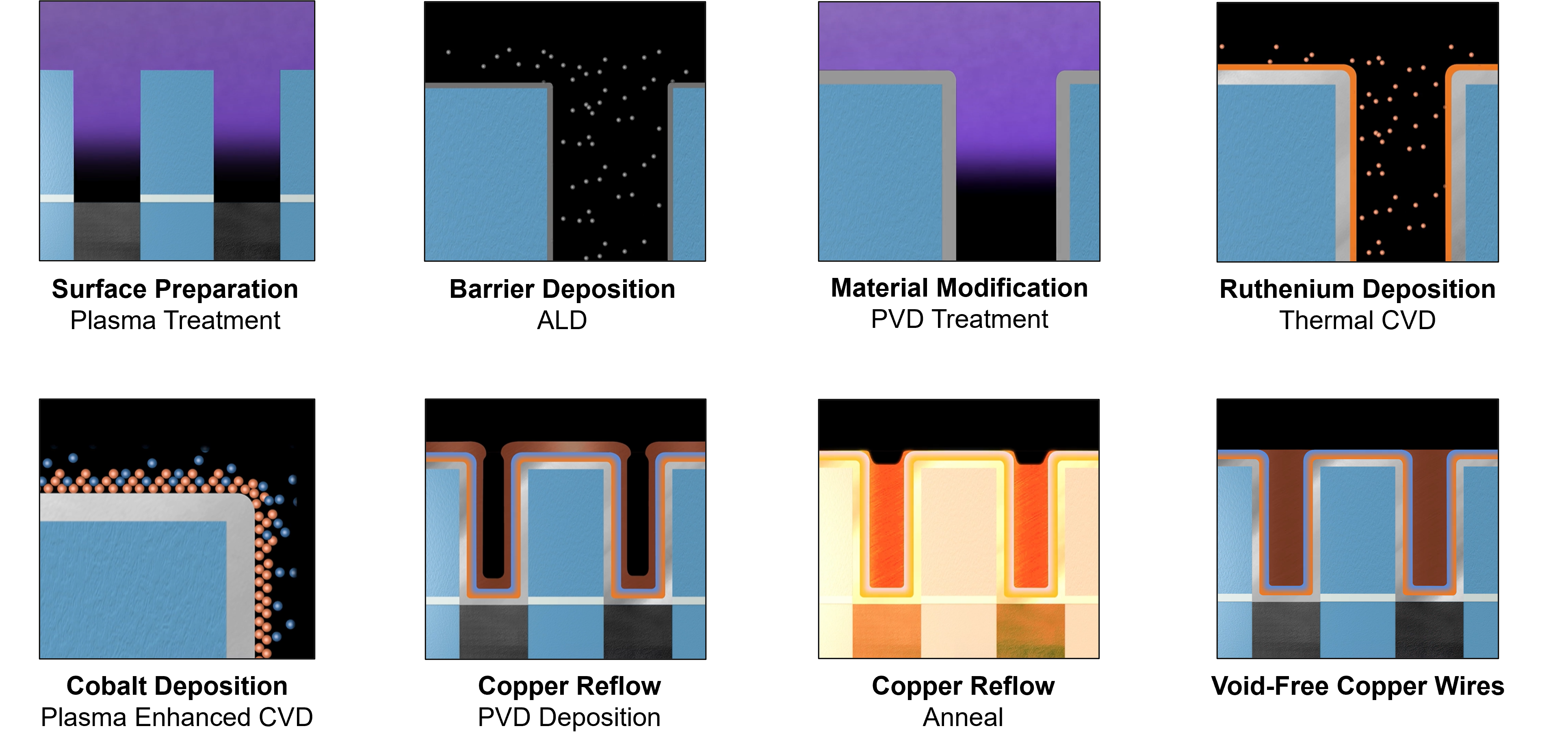
CuBS copper wiring flow Source: Applied Materials
3-Annealing
An annealing process is performed in a different system.
4-CMP
Then, a chemical-mechanical-planarization (CMP) process is performed using a CMP tool. The goal is to planarize the copper, liner, barrier and low-k cap layer.
5-Metal cap
A metal cap is formed on the structure.
6—BEOL Reliability
Finally, several reliability steps are performed.
What about BSPDN?
Traditionally, the BEOL copper interconnect structure handles the signal and power line functions. This structure is located on the frontside of the wafer. At advanced nodes, though, RC delay and IR power drops are still a problem.
There is a solution: a backside power delivery network (BSPDN). At the 2nm node and beyond, some but not all chips will incorporate a BSPDN. In BSPDN, the signal and power line functions are split into two pieces.
In BSPDN, a new interconnect-like structure is fabricated on the backside of the device. The BSPDN routes the power lines through the backside of the device. Meanwhile, the traditional BEOL interconnect structure remains intact on the frontside. But this structure is only used for signal routing in the device.
“There are two primary innovation paths for wiring at the most advanced nodes: 1) moving the power lines to the backside of the wafer to reduce power and increase logic density (BSPD); 2) extending copper wiring on the frontside of the wafer with materials engineering to reduce resistance and increase performance-per-watt,” Applied’s Thareja said.
“Our (VLSI) paper focuses on the latter,” Thareja said. “With BSPD schemes, there is a BEOL metal stack on both sides of the wafer. The signal wires are on the frontside of the wafer. These will be the thinnest wires that will leverage the most advanced technologies such as RuCo. The backside of the wafer will house a stack of wires for power delivery. These will be fatter wires that won’t need the newest scaling technologies.”