


Taiwan Firm Boosts U.S. Silicon Wafer Industry
Updated: GlobalWafers is shipping the first wafers from its two new and advanced silicon wafer manufacturing plants in the U.S.

By Mark LaPedus
In a major boost for the U.S. semiconductor industry, Taiwan’s GlobalWafers is shipping the first products from its two new and advanced silicon wafer manufacturing plants in the United States.
GlobalWafers’ new silicon wafer production facilities are located in two states--Texas and Missouri. In fact, the Texas-based facility is the most advanced silicon wafer production plant in the U.S.
In addition, GlobalWafers announced plans to increase its investments in the U.S. by another $4 billion. In total, the company plans to invest $7.5 billion in the U.S. Silicon wafers are the fundamental building material for the majority of semiconductors, which are vital components of all electronic devices. A silicon wafer serves as the foundation or the base material for a chip.
GlobalWafers’ announcements represent a major boost for the U.S. semiconductor industry. The U.S. produces only a small percentage of the world’s silicon wafers. Most silicon wafers, including leading-edge products, are produced in Asia. With GlobalWafers’ U.S. facilities, chipmakers in the U.S. now have a new and domestic source of supply.
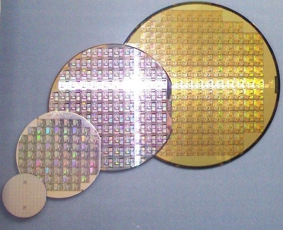
Silicon wafers of different sizes Source: Wikipedia
Silicon wafer landscape
The semiconductor industry has been making chips using silicon wafers since the 1950s. A silicon wafer is a round and thin product, which is used in the semiconductor manufacturing process to create chips. Based on high-purity silicon materials, these wafers serve as the substrate for a chip.
GlobalWafers is the world’s third largest silicon wafer maker, behind Japan’s Shin-Etsu and Japan’s Sumco. Siltronic (Germany), SK Siltron (Korea), Soitec (France) and others make wafers. Suppliers from China are also producing silicon wafers.
To make a silicon wafer, suppliers have used the same basic process since the 1950s. This process, known as the Czochralski (CZ) method, starts by pouring high-purity polycrystalline materials into a large cylindrical crucible. Then, a crystal silicon seed is added into the crucible.
This in turn forms a large silicon crystal ingot. The ingot is pulled from the crucible. Using a hi-tech saw, thin silicon wafers are sliced from the ingot. Each wafer has a thickness of around 1mm.

The Czochralski method Source: Wikipedia
Basically, in a facility, a silicon wafer supplier (i.e. Shin-Etsu, Sumco, GlobalWafers, etc.) produces silicon wafers at various diameter sizes, such as 150mm, 200mm and 300mm. Each wafer size is targeted for a different application.
Silicon wafer makers also develop different types of wafers. Epitaxial (epi) wafers and polished wafers are the most common types. Epi wafers are used by chipmakers to manufacture logic chips (GPUs, processors). Polished wafers are used by memory makers to make DRAMs and flash memories.
After the wafers are produced, they are sold to semiconductor manufacturers, such as Intel, Micron, TSMC, Samsung, SK Hynix, TI and others. At that point, semiconductor manufacturers will fabricate chips on top of these wafers in large manufacturing facilities called fabs. In other words, silicon wafers serve as the base material for chips.
Today, 90% of all silicon wafers are produced in Asia, according to the U.S. Department of Commerce. There are several silicon wafer production plants in the U.S. But the U.S. only produces a tiny percentage of the world’s wafers.
Nonetheless, the silicon wafer business is a cyclical and competitive market. For some time, this market has been in a slump. Worldwide silicon wafer shipments in 2024 decreased 2.7% to 12,266 million square inches, while wafer revenues contracted 6.5% to $11.5 billion over the same period, according to the SEMI Silicon Manufacturers Group (SMG).
In the first quarter of 2025, worldwide silicon wafer shipments reached 2,896 million square inches, up 2.2% from the like period a year ago, according to the SMG. Sequentially, shipments contracted 9% from the fourth quarter of last year. This was primarily due to the seasonality slowdown and accumulated inventory levels throughout the supply chain.
“Q1 2025 silicon shipments indicated a 6% year-over-year growth in 300mm, but showed a decline in 200mm and below wafer sizes,” said Lee Chungwei, chairman of SEMI SMG and vice president and chief auditor at GlobalWafers. “Despite an incremental increase in 300mm wafer shipments, demand for legacy devices remains weak, with inventory adjustments also contributing to a slowdown in shipments.”
GlobalWafers saves U.S. wafer biz
Meanwhile, years ago, the U.S. had a strong position in the silicon wafer business. That changed in 2016, when Taiwan’s GlobalWafers acquired the silicon wafer unit of U.S.-based SunEdison. The event was a blow for the U.S. semiconductor industry. SunEdison Semiconductor, formerly known as MEMC, was the last major U.S.-based silicon wafer maker.
In recent times, the U.S. government recognized that silicon wafers are a critical part of the semiconductor industry. Last year, GlobalWafers signed a non-binding preliminary memorandum with the U.S. government to obtain up to $400 million in funding under the CHIPS and Science Act. The funding was supposed to help GlobalWafers construct new silicon wafer manufacturing facilities in Texas and Missouri.
Reports have surfaced that GlobalWafers has yet to obtain any funding under the CHIPS Act, which is now in limbo. “Our CHIPS Act application has been submitted and is currently under review,” according to officials from GlobalWafers. However, the company recently obtained a $5 million grant from the Sherman Economic Development Corp. in Texas.
Nonetheless, in 2022, GlobalWafers broke ground on its new facilities in the U.S. In 2024, the company completed the construction of its new facilities.
In the first quarter of 2025, GlobalWafers shipped the first wafers from its new 300mm silicon wafer production facility in Sherman, Texas. That facility is the most advanced high-volume 300mm silicon wafer production facility in the U.S. Products from this facility will be used in the manufacturing of advanced logic and memory devices.
The company is also ramping up the first wafers from its new 300mm silicon-on-insulator (SOI) wafer production facility, which is located in St. Peters, Mo. SOI wafers from this facility will be used to develop chips across the defense and aerospace sectors.
At present, GlobalWafers is still in the qualification stage in both U.S.-based plants. The goal is to move into mass production in the second half of 2025.
At some point in the future, GlobalWafers plans to add two new phases to its existing facilities in Sherman. “On the three-year anniversary of our decision to build GWA (GlobalWafers America), I am pleased to announce GlobalWafers’ intention to expand our current U.S. investment by another $4 billion to reach $7.5 billion,” said Doris Hsu, chairperson of GlobalWafers, at a recent event.
“At this stage, we do not yet have a fixed timeline for future expansion phases at our U.S. site, as our current focus is on ramping up the initial phases. That said, we do sense strong interest from customers in locally sourced supply, and the company remains open to further expansion, with timing to be adjusted based on market demand,” according to officials from GlobalWafers.
GlobalWafers maintains 18 manufacturing and operational sites spanning three continents and nine countries.