
Test Challenges Grow For DRAMs and HBM
ATE giant Advantest discusses the trends and challenges in testing DRAMs and HBM.

By Mark LaPedus
Jin Yokoyama, senior director and memory product marketing manager at Advantest, sat down with Semiecosystem to discuss the trends and challenges in testing DRAMs and high bandwidth memory (HBM).
Semiecosystem: Who is Advantest and what is the company’s charter?
Yokoyama: As the automated test equipment (ATE) leader in the semiconductor industry, we develop system-on-chip (SoC) testers, memory testers, and system-level testers, as well as peripheral equipment and boards. Our memory test systems are optimized for volume production of memory semiconductors, a market where low-mix/high-volume production is the norm, and features industry-best parallelism (i.e., the ability to test a large number of semiconductors at the same time).
We offer a range of memory test systems, including DRAM, NAND and emerging NVM (non-volatile memory) testers. Our broad product portfolio enables us to provide one-stop, turnkey solutions optimized for each customer’s needs.
Semiecosystem: Advantest supplies ATE for both logic and memory devices. Let’s focus on memory devices, particularly DRAMs. DRAMs, which have been around for ages, are the chips that provide the main memory functions for computers, smartphones and other systems. Why is it important to test DRAMs before these devices end up in systems?
Yokoyama: As you likely know, DRAM devices play an important role in data storage, allowing your computers, smartphones, and tablets to process data quickly and efficiently. As such, DRAM has a significant impact on the overall performance of the devices we use, since the CPU communicates directly with the DRAM device to access data needed to make calculations. It is critical to test DRAM devices in advance to ensure the devices are reliable and operate as expected in the end-use environment.
Semiecosystem: In general, how do we test the latest DRAMs? Isn’t there a test flow involved here? Can you briefly describe the basic test flow for DRAMs and each step?
Yokoyama: Typically, for DRAM devices, the test flow starts with wafer-level test. At the wafer level, our test systems apply memory test algorithms at varying speeds to test DRAM performance. The DRAM device is then tested again after it is assembled into a package. The final test stage runs tests at operational speed to confirm whether the device processes data correctly and meets end-use requirements.
Semiecosystem: Over the years, DRAMs have become more complex. What are some of the technology trends that you see with current and future leading-edge DRAMs?
Yokoyama: We see a myriad of trends emerging as DRAM technology evolves. DRAM devices are playing a critical role across a variety of applications, including artificial intelligence (AI)/high-performance computing (HPC), data centers, smartphones, AI PCs, and video game consoles.
The growth of AI, specifically, has led to an increase in demand for DRAM devices with higher per-pin speed, higher bandwidth, and low latency. Meanwhile, data centers and AI edge applications require devices to integrate new industry standards for speed and power consumption, including GDDR7, LPDDR6, and HBM4. These devices must also have lower output levels to maintain accuracy and higher operational efficiency to reduce cost.
We also see the trend of miniaturization and the shrinking of bit cells. There is a shift in size to 3000 devices under test (DUTs) per 300mm wafer, leading to higher density that makes DRAM devices more vulnerable to defects. This means that these devices will likely require more tests and screening to meet demands for quality and reliability. Further densification of tester resources and technology will be necessary to accommodate device miniaturization trends.
Semiecosystem: What are some of the test challenges with the latest DRAMs?
Yokoyama: The increasing speed of these devices certainly presents a challenge in the test process. Speed performance requirements for at-speed interface testing on DRAM devices are increasing from 4.5 Gbps to over 10 Gbps, requiring high-performance test equipment to run test algorithms at high operational speeds.
We also need test systems that can test more devices in parallel to maintain lower costs. This requires highly specialized probe card technology that can handle high-speed testing. Massive levels of parallelism will be vital, as the industry trends toward requiring only one touchdown per wafer. Miniaturizing DRAM devices also makes them more susceptible to defects, requiring more thorough testing in the form of burn-in test at the wafer and package levels. Moreover, thermal requirements for DRAM devices continue to rise alongside demands for higher power and bandwidth capacity, and the complexity of integrating DRAM in 2.5D/3D packaging poses its own set of unique test challenges.
In the DRAM market, where high bandwidth and high performance continue to increase, Advantest recently introduced a next-generation ultra-high-speed solution, the T5801. This cutting-edge platform is engineered to support the latest advancements in high-speed memory technologies – including GDDR7, LPDDR6, and DDR6 – critical to meeting the growing demands of AI, HPC, and edge applications.
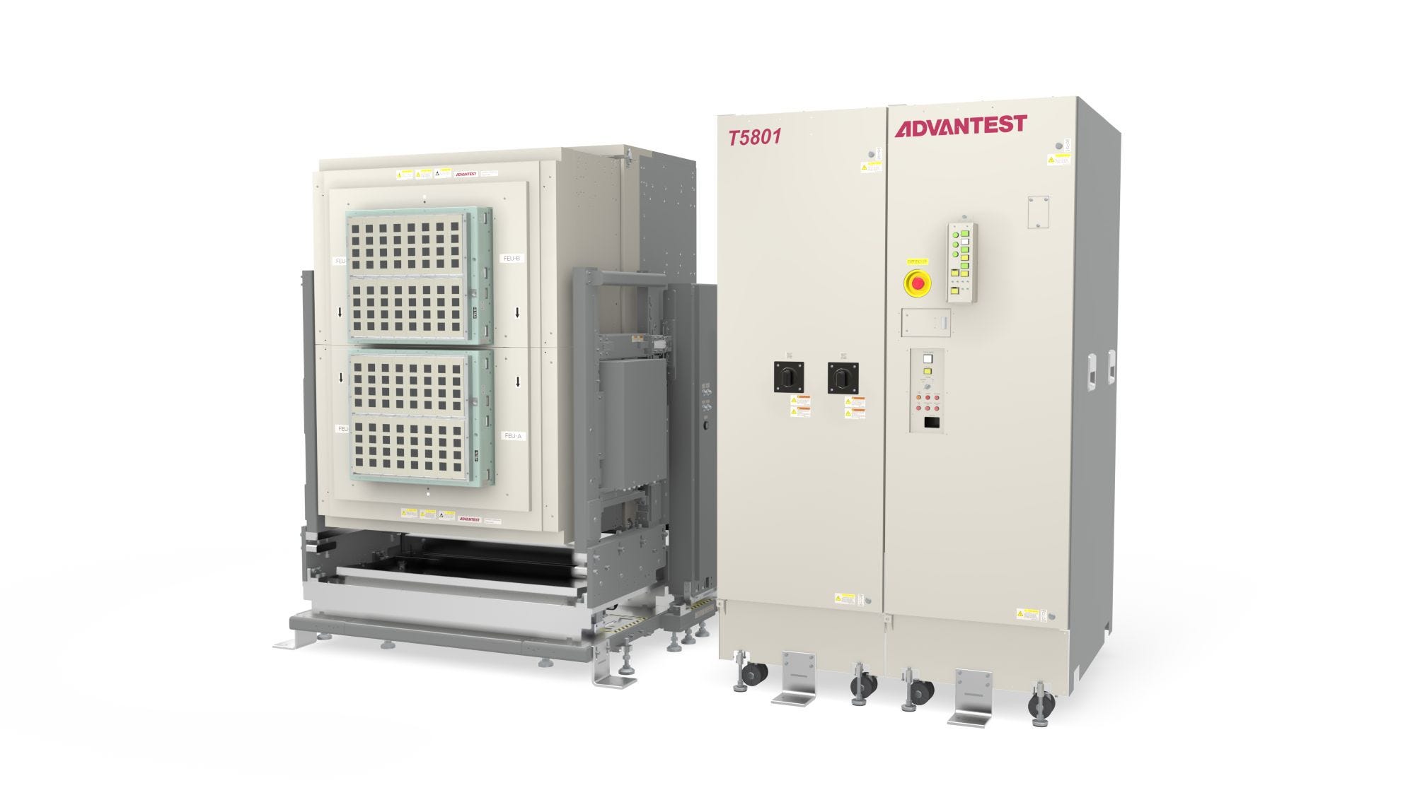
The T5801 Ultra-High-Speed DRAM Test System is a cutting-edge platform that supports the latest advancements in high-speed memory technologies, including GDDR7, LPDDR6, and DDR6. (Source: Advantest)
Semiecosystem: At each new generation or node, DRAM suppliers have been incrementally shrinking the cell size of these devices. Suppliers are shipping DRAM at the 1-beta node, with 1-c and/or 1-gamma in the works. Does this present more challenges in terms of test? If so, how? Will test times and costs increase at each node?
Yokoyama: As mentioned above, the shrinking of DRAM nodes presents challenges, as the increasing density makes the device more susceptible to defects. As the device’s circuitry and processing become more refined, its voltage levels and power consumption decrease. This requires specialized mechanisms and equipment to maintain the test system’s accuracy when handling such small amplitudes.
This is also important in improving throughput as test times become longer due to increased capacity size and miniaturization. In addition, various memory functions and enhanced error-correction code (ECC) are required to improve reliability with miniaturization, so we must work to support testing of these functions.
Question: High bandwidth memory (HBM) is a hot topic. Targeted for AI applications, HBM is a stack of DRAM dies, which are connected using through-silicon vias (TSVs). What are some of the technology trends and challenges that you are seeing with HBM?
Yokoyama: AI and HPC devices are demanding higher and higher processing speeds to power advanced applications like large-language models (LLMs). HBM consists of multiple DRAM chips stacked vertically. This structure allows for faster and more efficient data transfer with a smaller footprint, which is why HBM plays a key role in data centers. Of course, these HBM devices are incredibly complex and pose various challenges during testing. With multiple DRAM ICs stacked on top of each other, these devices are extremely dense and produce a lot of heat, which poses a risk to the structure of the device. Test systems must be equipped with the proper thermal-management capabilities and refined handler/probe equipment needed to monitor potential hotspots and dissipate heat.
The density of device circuitry and the number of DRAM devices stacked is increasing with each generation of HBM, moving from 8 stacks to 12, 16 and even 24 stacks. This has led to longer test times, especially as HBM migrates much faster than traditional memory technology transitions by generation. Higher interface speeds and higher bandwidth of HBM devices also mean high test speed and an increased load on peripheral circuits, requiring high-speed probing technology. Moreover, increases in power supply and current capacity require scalability.
The 2.5D/3D packaged structure of HBM devices also poses significant challenges, requiring thorough testing before the devices are packaged together. More and more manufacturers are looking to utilize die-level test, i.e., testing individual die after the wafer has been diced, to ensure that the DRAM ICs function properly before they are stacked into an HBM device and packaged, increasing overall yield and reliability. “Known-good die” or KGD testing, as it’s sometimes called, helps to prevent manufacturers from assembling packages containing defective die. If even one die in a stack is defective, then the entire package must be disposed of at great cost to the manufacturer.
Semiecosystem: In general, what are the main test challenges for HBM?
Yokoyama: To summarize the answer provided above, the main test challenges of HBM are:
•Increasing device complexity (2.5D/3D packaging, chiplets, etc.)
•Migrates much faster than traditional memory technology transitions by generation
•Next HBM generation leads to higher density and more TSV stacking
•Next HBM generation leads to higher bandwidth and per-pin speed
•Thermal management during test
Semiecosystem: HBM requires a complex test flow. I believe the HBM testing process involves two parts—before stacking and after stacking. (See below for HBM test flow.) Can you explain the testing process in the before stacking phase? What types of test systems and/or test technologies are required here?
Yokoyama: The test process for DRAM ICs destined for HBM isn’t all that different from DRAMs that will be used in PCs, tablets, or other devices. The process begins with wafer-level burn-in test where varying levels of high heat and high voltage are applied to the wafer to stress the devices and help engineers identify failing devices early in the test process.
Specialized burn-in boards are needed to run this type of test, and Advantest’s B6700 burn-in test system can test multiple burn-in boards in parallel at speeds up to 10 MHz. Next comes wafer-level test, where the test algorithm can be applied at both lower speeds and operational speeds to check device functionality. Due to the advanced packaging requirements of HBM devices, there has been a push in the industry for KGD testing. This requires highly specialized equipment like die-level handlers that can handle the bare die with precision and care in this fragile stage. Advantest’s T5835 can perform KGD test, offering test coverage for next-generation memory chips such as DRAM for advanced HBM devices.
Semiecosystem: Can you explain the testing process during the after stacking phase?
Yokoyama: After the wafer is cut into individual die, the devices are incredibly fragile. Because of this, we are seeing advancements in automated handling systems for secure stacking and assembly of fragile die into stacked devices or 2.5D/3D packages.
Manufacturers utilize TSVs as a method of heterogeneous integration to connect multiple die into a single stacked structure. Once they are stacked and connected, the bonded interconnects between these die must be tested to ensure that the alignment is correct.
This requires advanced, sophisticated equipment to differentiate between the different die stacked on top of each other, especially as the stacks get higher and higher as manufacturers look to integrate more DRAM devices into the same stack to meet the demands for high-speed, higher-performance devices. Then, in the case of HBM, manufacturers also need to test how the DRAM devices integrate with the logic devices they are bonded and packaged with. They must ensure that all of the devices in the package can perform at the same level with similar processing speeds.

HBM test flow (Source: Advantest)
Semiecosystem: Are there any test challenges when the industry migrates to HBM4?
Yokoyama: The greatest challenge we will see is the rising complexity of HBM4 devices. HBM4 base logic wafers are being made at leading-edge logic foundries for use in high-performance data centers to power AI edge applications. This will make the supply chain more complex, and the requirements and manufacturing and testing processes for DRAM manufacturers, foundries, and SoCs will also become more complex as a result. So, more advancements will have to be made in test process optimization in the future to support the next generation of HBM.