
TSMC, China Foundries Ramp Up New Fabs For Mature Nodes
Several foundry vendors are aggressively expanding their fab capacities at the mature, or trailing-edge, nodes.

By Mark LaPedus
Despite sluggish business conditions in the marketplace, several foundry vendors are aggressively expanding their fab capacities at the mature, or trailing-edge, nodes.
Over the next year, there are at least four foundry vendors that have major fab expansion plans in the important but overlooked mature node segment. TSMC, the world’s largest foundry vendor, is ramping up production in a new fab in Japan, which will manufacture chips at relatively mature process nodes. In addition, HuaHong Group, NexChip and SMIC are gearing up for production in their new mature-node fabs in China, according to TrendForce, a research firm. In fact, China is taking steps in hopes of dominating the mature-node foundry market over time.
Other foundry vendors are also building up new mature-node fab capacity. Generally, trailing-edge, or mature, process nodes are older technologies that have been around for years, but they are still important. Chips that are manufactured using mature processes are still used in every electronic system today. These systems include appliances, cars, computers, medical equipment, smartphones, telecommunication gear, wireless infrastructure systems and other products.
A process is a term used in the semiconductor industry that describes the design rules and recipes used in manufacturing a given chip line. In the semiconductor world, there are different process nodes and each one is represented by a number and a unit of measurement. A lower node number means that the process, and the chip product, are more advanced.
Foundry vendors use leading-edge processes to make the most advanced chips. These processes can range anywhere from the so-called 16nm/14nm to the 3nm nodes. The 2nm process and the nodes below that number are in R&D.
Mature, or trailing-edge, processes involve the process nodes at 20nm and above (i.e. 28nm, 40nm, 55nm, 65nm, 90nm, etc.). In recent times, it’s been a relatively difficult period in this segment for many semiconductor suppliers and foundries.
Today, AI chip demand is enormous. But on the flip side, there has been sluggish demand for chips in the automotive, consumer and industrial sectors. A large percentage of chips used in these sectors are built using mature processes. Many of these chips are fabricated in foundries. Thus, over the last year or so, foundry vendors have seen lackluster demand and price pressures at the more mature nodes.
Then, for some time, China’s domestic foundry vendors have been aggressively building new fabs, most of which are targeted for the production of chips at more mature processes. This in turn has caused overcapacity in some mature-node areas, thereby contributing to the lackluster business conditions.
At present, China has some 44 wafer fabs in operation, according to TrendForce. In addition, there are 22 wafer fabs under construction in China, according to the research firm. Most of the current and future facilities are mature-node fabs.
In any case, the new fab capacity additions could prolong the worldwide slump in the mature-node segments well into 2025 and perhaps beyond.
In total, revenue for semiconductor foundry services declined by 11.7% in 2023 to $115.2 billion, according to Gartner. The decline was due to a slowdown in demand for chips in the smartphone, PC and consumer electronic segments, according to Gartner. 2024 is a recovery year for foundry vendors. But some markets are recovering faster than others. The foundry industry is expected to grow by 10% this year, according to some estimates.
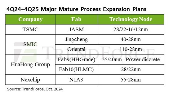
In the foundry business, there are several major mature process fab expansion plans. JASM is TSMC’s new fab venture in Japan. SMIC, HuaHong and NexChip have new fabs in place in China. Source: TrendForce
Manufacturing landscape
From a manufacturing standpoint, there are three types of companies in the semiconductor industry—integrated device manufacturers (IDMs), foundry vendors, and fabless design houses. IDMs design their own chips and manufacture them in their own fabs. Foundry vendors manufacture chips for other companies in fabs. Fabless design houses don’t have fabs—they design their own chips and have them manufactured by foundry vendors.
To manufacture a chip line, IDMs and foundry vendors obtain a round and thin wafer. The most common wafer sizes are 200mm and 300mm in diameter. Then, a semiconductor manufacturer takes the wafer and subjects it to various process steps in a fab, which in turn produces the desired chip line.
Simply put, fabs that process 300mm wafers are called 300mm fabs. Fabs that process 200mm wafers are called 200mm fabs.
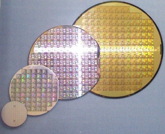
Silicon wafers at various sizes Source: Wikipedia
In a fab, foundry vendors manufacture a wide range of chips using either leading- or trailing-edge processes. Some foundry vendors provide leading-edge processes for their customers. Others offer trailing-edge processes. Some offer both.
As stated above, for foundry vendors, leading-edge processes range anywhere from the 16nm/14nm to the 3nm nodes. Typically, chips based on these advanced processes are produced in 300mm fabs. Three foundry vendors--Intel, Samsung and TSMC--provide the most advanced processes in the foundry market.
Meanwhile, mature processes involve the 20nm process nodes and above. Chips produced using trailing-edge processes can be manufactured in 100mm, 150mm, 200mm or 300mm fabs. GlobalFoundries, HuaHong Group, NexChip, Skywater, SMIC, Tower, TSMC, UMC and other foundry vendors are all capable of manufacturing chips using mature processes.
At the end of 2022, there were a total of 167 fabs processing 300mm wafers worldwide, according to Knometa, a research firm. Plus, in 2022, there were 224 200mm fabs worldwide, according to SEMI.
For advanced manufacturing processes, Taiwan leads with a 68% global capacity share in 2023, followed by the U.S. (12%), South Korea (11%), and China (8%), according to TrendForce. For mature processes, Taiwan leads with a 44% global capacity share in 2023, followed by China (31%), South Korea (6%), and the U.S. (5%), according to TrendForce.
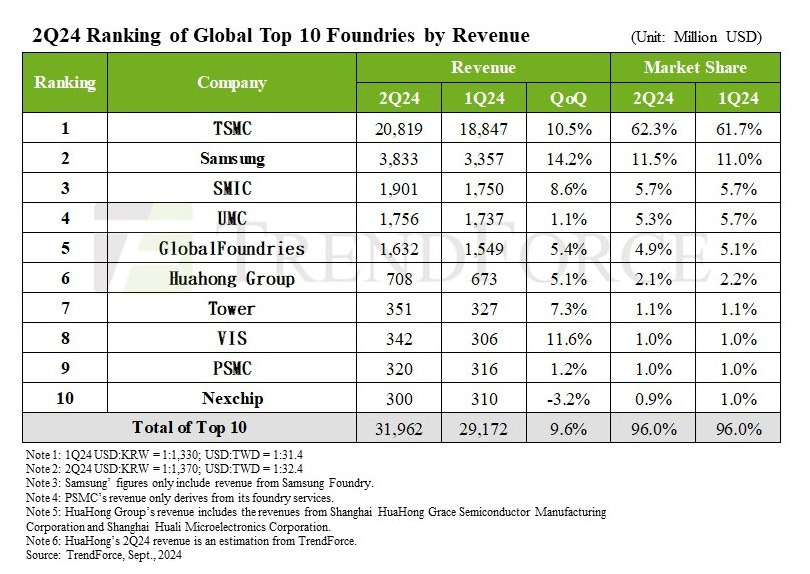
In the second quarter of 2024, TSMC remained in first place in the overall foundry rankings with a dominate 62.3% market share, followed in order by Samsung (11.5% share), SMIC (5.7%), UMC (5.3%), GlobalFoundries (4.9%), HuaHong Group (2.1%), and Tower (1.1%), according to TrendForce.
Leading-edge vs trailing-edge
Today, meanwhile, the foundry industry is a tale of two markets. Demand for leading-edge processes is up, but the mature process market is relatively slow.
For some time, demand has been robust for the most advanced processes, namely the 4nm and 3nm nodes. For example, Nvidia is experiencing overwhelming demand for its GPU chips, which are used in AI applications. Based on a 4nm process, Nvidia’s GPUs are manufactured by TSMC. In addition, TSMC also manufactures Apple’s application processors for the iPhone. Apple’s latest processors are based on a 3nm process.
“The 5/4nm and 3nm nodes, driven by AI servers, PC/notebook, HPC chips, and new smartphone SoCs, will see full capacity utilization through the end of 2024,” according to TrendForce. “Although the demand for 7nm/6nm processes has been weak for the past two years, new demand is anticipated to emerge between the second half of 2025 and 2026, driven by the transition plans for RF/WiFi processes in smartphones.”
In 2025, the leading-edge processes, including 7nm, 6nm, 5nm, 4nm and 3nm technologies, are expected to contribute 45% of global revenue for foundry vendors.
It's a different story for the mature process segments, which involve the 20nm node and above (i.e. 28nm, 40nm, 55nm, 65nm, 90nm, etc.). These mature processes are used to make a wide range of chips, including analog devices, automotive chips, display driver ICs, MEMS, power semiconductors, RF products and others.
Many of these markets have been in the doldrums in 2023 and 2024. Take the automotive market for example. During the pandemic, there were acute shortages of chips for the automotive market. Over time, chip vendors in the automotive sector were able to catch up and meet demand.
In recent times, though, there has been more chip supply than demand in the automotive sector. The same is true for many of the industrial and consumer chip markets. Many chip vendors in these and other markets use foundries. As a result, foundry vendors have seen lackluster demand for chips at the more mature nodes. In this segment, fab capacity utilization rates among foundries have hovered around the 70% range or lower. In comparison, fab utilization rates were hovering about 100% during the pandemic.
In the second half of 2024, business appears to be picking up. “Mature nodes of 28nm and above are experiencing only a moderate recovery, with average capacity utilization increasing by 5% to 10% in the second half of this year compared to the first,” according to TrendForce. “Looking ahead to overall pricing trends in 2025, mature process pricing is expected to remain under pressure due to average capacity utilization remaining below 80% and new capacity still needing orders to fill.”
New fabs
Despite lackluster business conditions, several companies are ramping up new fabs, which will produce chips at more mature nodes. For example, in the fourth quarter of 2024, TSMC moved into production in its fab venture in Japan. The venture, called Japan Advanced Semiconductor Manufacturing (JASM), is located in the Kumamoto Prefecture. Denso, Sony and Toyota are minority shareholders in JASM. (See chart above)
With a monthly capacity of 55,000 wafers, JASM will produce chips using 28nm/22nm and 16nm/12nm processes. JASM will produce chips for automotive, industrial, consumer and HPC-related applications. “Volume production was started this quarter and we are confident to deliver the same level of manufacturing quality and reliability from our fab in Kumamoto, as from our fabs in Taiwan,” said C.C. Wei, chairman and chief executive of TSMC, in a recent conference call.
TSMC plans to build a second fab in Kumamoto, with production slated by 2027. The goal is to produce 6nm/7nm chips. The overall investment in JASM will exceed $20 billion with strong support from the Japanese government.
Other foundry vendors from Taiwan are also building new fabs. Besides Taiwan, China is also in the midst of a massive fab expansion campaign.
The Chinese government would like to produce chips at both trailing- and leading-edge nodes. But not long ago, the U.S. launched a trade war against China. As part of those efforts, the U.S. has initiated various export controls and sanctions against China. In effect, China is unable to obtain various leading-edge fab equipment, thereby preventing domestic foundries from moving to the world’s most advanced nodes.
The U.S.-backed sanctions do not pertain to more mature chip-making equipment from the multinationals. In fact, China is buying a plethora of this equipment from the likes of ASML, Applied Materials, KLA, Lam and others.
That’s not stopping China from advancing its semiconductor industry. Today, SMIC, China’s largest foundry vendor, is shipping chips based on an internally-developed 7nm process, with 5nm in R&D. That represents China’s most advanced process. Still, SMIC is roughly two generations behind TSMC and Samsung.
China and its domestic foundry industry are also making a push to dominate the mature-node technologies, and for good reason. In China, there is huge demand for chips at mature processes. China itself has a significant number of domestic car makers, PC vendors, smartphone companies and telecom firms. All of these applications require trailing-edge chips.
China buys many of these chip types from multinational semiconductor companies. But a growing number of these chip types are designed by various China-based IC design houses. The Chinese government would prefer these chips manufactured by China’s domestic foundries, not the multinational vendors. In fact, some China-based foundries are capturing business from chips designed in the domestic market. As a result, some domestic foundries are recovering faster than their multinational rivals in the mature-node segment.
For this reason and others, China-based foundries are set to drive the bulk of mature process capacity growth in 2025, according to TrendForce. SMIC, for example, is ramping up fabs in Lingang (Shanghai) and Beijing. The Beijing fab is set to produce 40nm to 28nm devices.
In 2021, SMIC and China’s Lin-Gang FTZ Administration entered into a joint fab venture in Lingang. The fab, to cost $8.87 billion, will have a production capacity of 100,000 300mm wafers per month, focusing on 28nm processes and above.
Meanwhile, China’s HuaHong Group is ramping up two facilities--Fab9 and Fab10. The HuaHong Group is a specialty foundry vendor that focuses on analog/power management, embedded memory, image sensors, power semiconductors, RF and other technologies.
The company is readying Fab9. "Construction of our second 12-inch production line is progressing at a fast pace and is expected to enter trial production by the end of this year,” said Tang Junjun, president and executive director of the HuaHong Group.
NexChip, meanwhile, is also ramping up a new fab, dubbed N1A3. NexChip focuses on power management, embedded memory, high-voltage and other processes. Located in China, NexChip is a joint venture between China’s Hefei Construction Investment Holding and Taiwan’s Powerchip (PSMC).
More processes
Other foundry vendors are also expanding their efforts in the mature process space. South Korea’s SK keyfoundry has expanded its high-voltage foundry services portfolio with the launch of its high-voltage integrated circuit process technology. The company is the logic foundry subsidiary of SK Hynix.
Meanwhile, Germany’s X-FAB Silicon Foundries, an analog/mixed-signal and specialty foundry, has introduced additional optoelectronic device options. Leveraging the company’s 180nm XS018 CMOS semiconductor process, the company has expanded its high-performance photodiode offerings.