


What Ever Happened To Gallium Oxide Power Semis?
Gallium oxide power devices potentially outperform GaN and SiC, but the technology remains in R&D.

By Mark LaPedus
For years, several companies, R&D organizations and universities have been working on power semiconductors built around gallium oxide, a promising technology that could potentially outperform today’s power devices based on gallium nitride (GaN), silicon carbide (SiC) and silicon.
So far, several entities have demonstrated various devices using gallium oxide (Ga2O3), but products based on this technology have not been commercialized or put into production. And it’s still unclear when gallium oxide devices will move into production amid ongoing challenges with the technology.
Still, several entities continue to pursue gallium oxide devices, and for good reason. Still in R&D, power semiconductors using gallium oxide materials exhibit a number of impressive characteristics. On paper, Ga2O3 devices can potentially withstand higher voltages with less resistance than the two rising stars in today’s power semiconductor market--GaN and SiC.
Power semiconductors aren’t new and have been around for years. Power semiconductor devices are used in nearly every system, including appliances, cars, chargers, computers, smartphones, solar panels, trains, wind turbines and others. In general, power semiconductors are specialized devices that can withstand higher voltages and currents with lower losses in a system, according to Power & Beyond, a technology website. Simply put, these devices help make a system more efficient.
For years, power semiconductors built around traditional silicon materials have dominated the market. But two relatively new device types, GaN- and SiC-based power semiconductors, have made inroads in the market, sometimes at the expense of the silicon-based devices.
Both GaN- and SiC-based devices fall under a general category called wide bandgap semiconductors. Wide bandgap devices can operate at higher voltages, temperatures and frequencies, as compared to traditional silicon-based products.
Gallium oxide is considered an ultra-wide bandgap technology, which, in some respects, have better specs than GaN, SiC and silicon. That’s why there is so much interest in gallium oxide. Here are just some of the entities working on gallium oxide devices:
*At the upcoming 2024 IEEE International Electron Devices Meeting (IEDM) in San Francisco, a group comprised of Virginia Tech, the U.S. Naval Research Laboratory and Novel Crystal Technology (NCT) will present a paper on a new breakthrough with gallium oxide devices.
*Japan recently announced a new gallium oxide research project.
*The U.S. Advanced Research Projects Agency-Energy (ARPA-E) is funding the development of the technology.
*Gallox Semiconductors, the first U.S.-based startup focused on the commercialization of gallium oxide devices, has emerged.
*Germany has funded a new project in the arena.
*China is working on gallium oxide wafers and devices.
Ga2O3 junction-gate field-effect-transistor (JFET). Source: Virginia Tech, the U.S. Naval Research Laboratory, Novel Crystal Technology (NCT)
Power semi landscape
The power semiconductor market, sometimes called power electronics, is a large and important business that often flies under the radar. In total, the power electronics market, including discretes and modules, was worth $23.8 billion in 2023, and is expected to grow to $35.7 billion by 2029, according to the Yole Group, a market research firm.
Power semiconductors are used in nearly every electronic system. “Power semiconductors supply and control electricity used to run motors and charge batteries by converting electric power from AC to DC and adjusting voltages to appropriate levels,” according to Yole.
In addition, these devices are used to control the flow of electricity in systems, while reducing the power losses during operation. And unlike conventional chips like AI devices and processors, power semis can withstand higher voltages and currents with lower losses in systems.
Power semiconductors are also designed to perform amplification or switching operations in systems. In amplification, the idea is to convert a small amount of electricity into a large amount in a system. These devices also serve as power transistors in a system. A transistor is a tiny structure that acts like a switch. “Switching is the act of turning ‘ON’ and ‘OFF’ large current and high voltage electricity with only a small amount of electric power,” according to Sanken Electric, a power semiconductor supplier.
There is no one power semiconductor type that handles all applications. In fact, a number of power semiconductor suppliers sell a multitude of different products with a wide variety of specifications. Each device type works within a specific voltage, frequency and temperature range. And each device type is targeted for a specific application based on those specifications.
Generally, power semiconductors are categorized into different product families, including power MOSETs, IGBTs, GaN power devices and SiC MOSFETs. There are many other power device families as well.
The power MOSFET is considered the entry-level product in the power semiconductor world. Power MOSFETs incorporate traditional silicon materials in the device structure. For years, power MOSFETs have dominated the landscape in the low- to mid-range markets. These devices are used in applications that range from 25 to 900 volts. Applications include appliances, chargers, servers and telecom gear.
Insulated-gate bipolar transistors (IGBTs) are used in mid-range to high-end applications. Like power MOSFETs, IGBTs incorporate traditional silicon materials in the device structure. IGBTs are used in 1,200-volt to 6.6-kilovolt applications. These include appliances, cars, motor control units and solar inverters.
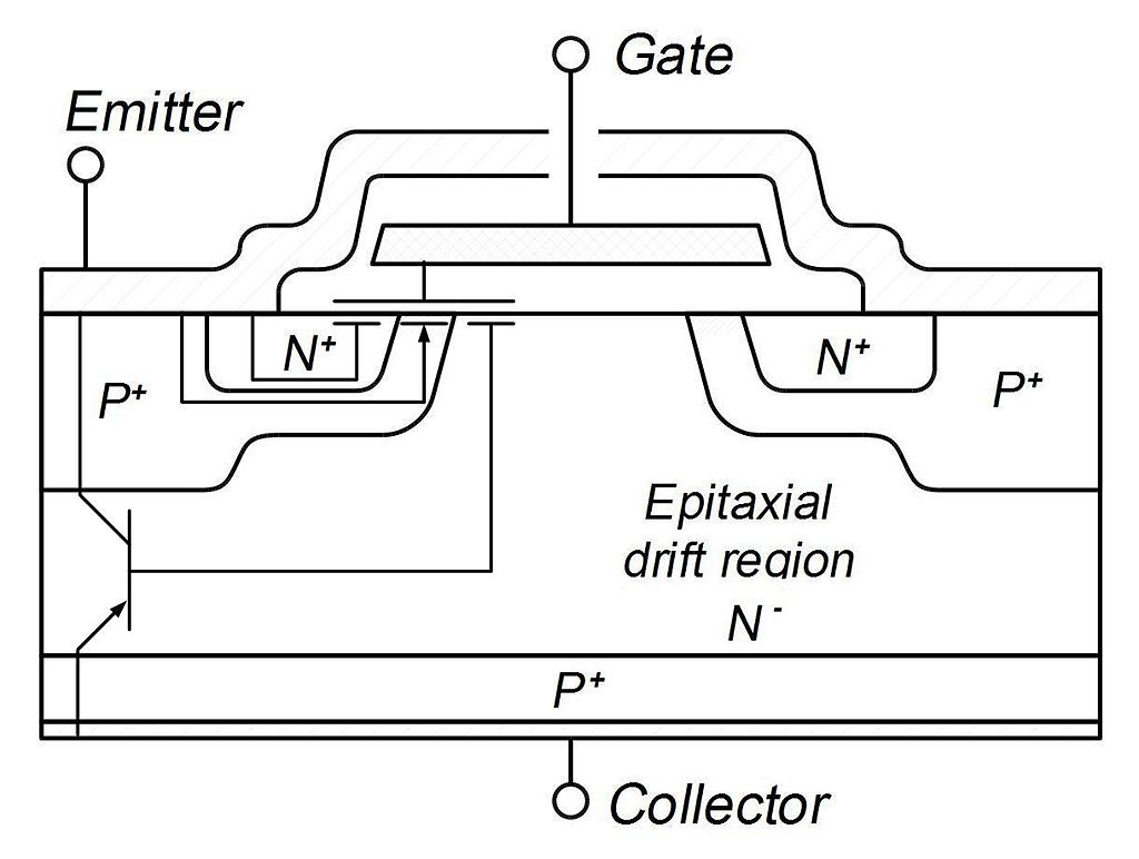
Cross-section of a typical IGBT Source: Wikipedia
Both power MOSFETs and IGBTs are not new and have been around for decades. They are relatively inexpensive and widely used in the market. But they are also reaching their physical limits, which in turn is driving the demand for a new class of power semiconductor devices based on two material types--GaN and SiC.
GaN and SiC are considered wide bandgap semiconductor materials. Silicon has a band gap of 1.12 eV, while SiC and GaN are rated at 3.26 and 3.4 eV, respectively. The properties of wide bandgap materials enable devices to operate at higher voltages, temperatures and frequencies, as compared to silicon-based power MOSFETs and IGBTs. Generally, wide bandgap devices are smaller, faster and more efficient than their silicon-based counterparts.
A GaN-based power semiconductor incorporates GaN materials in the device structure. Generally, GaN-based power devices are used in 100- to 900-volt applications. Power Integrations, a supplier of power semis, recently launched a 1700-volt GaN switch IC.
A SiC-based power semiconductor, meanwhile incorporates SiC materials in the device structure. SiC-based devices are used in 600-volt to 10-kilovolt applications.
Both GaN- and SiC-based power devices are widely used in the market today. “The power device market is led by silicon, with SiC gaining ground in EV and industrial applications, while GaN serves consumer power supplies and e-mobility. Gallium oxide could become a future contender,” said Milan Rosina, an analyst at Yole.
Gallium oxide pros and cons
In R&D, several entities are working on ultra-wide bandgap technologies. Gallium oxide, one of several ultra-wide bandgap technologies, has gained interest in the market. Gallium oxide, an inorganic compound, is a white powder that consists of rod-shaped crystals, with the β-phase being the dominant crystalline phase, according to Indium, a materials supplier.
Gallium oxide boasts a band gap of 4.8 eV, with a critical field value of 8 MV/cm. That represents 3,000 times that of silicon, more than 8X that of SiC, and more than 4X that of GaN. So on paper, ultra-wide band gap semiconductor devices based on gallium oxide can withstand higher voltages with a lower resistance than GaN, SiC, and, of course, silicon.
The problem? There are several challenges with gallium oxide, preventing the devices based on the technology from moving into production.
For one thing, gallium oxide has poor thermal conductivity, which could cause a device to overheat. In addition, there is no intrinsic p-type doping technique for gallium oxide. This impacts the device structure and limits the applications for the technology. In chip production, doping introduces impurities into a semiconductor. This in turn modulates the properties of a device.
On the bright side, gallium oxide wafers are easier to produce, as compared to both GaN and SiC substrates. But today, gallium oxide is produced on 2-inch wafers, with 6-inch (150mm) substrates in the works. It’s difficult to produce cost-effective devices on smaller wafer sizes.
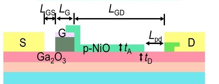
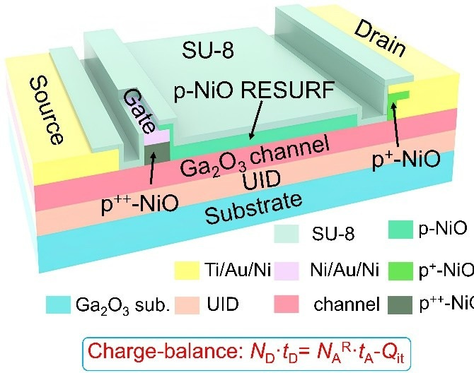
Nonetheless, the industry is beginning to make progress with the technology. At IEDM, the team of Virginia Tech, U.S. Naval Research Laboratory and NCT will present a paper that represents a possible breakthrough for gallium oxide. Researchers built a lateral Ga2O3 junction-gate field-effect-transistor (JFET), employing high p-doped NiO for E-mode operation, and hybrid-drain structures for electric field management. (See image above and below)
The device features breakdown voltages exceeding 10kV, and specific on-resistance values of 92 and 703mΩ·cm2 for thick- and thin-channel designs, respectively. “The devices demonstrated not only the best figures-of-merit (FOM) of all >3kV UWBG transistors, but also the first 250◦C operation and 3kV reliability data of all high-voltage transistors other than Si and SiC devices,” said Yuan Qin, a research scientist at the Department of Electrical and Computer Engineering at Virginia Tech, in the paper. Others contributed to the work.
Another view of a Ga2O3 junction-gate field-effect-transistor (JFET). Source: Virginia Tech, the U.S. Naval Research Laboratory, Novel Crystal Technology (NCT)
Developments in Japan
Others are also working on the technology. In some respects, Japan is leading the pack in the gallium oxide arena. Two Japanese companies, Flosfia and NCT, are working on the technology.
Last year, Flosfia and JSR developed a new iridium-based film deposition material as a solution for mass production of iridium gallium oxide. This material enabled the world’s first p-type power semiconductor developed using a corundum-type gallium oxide compound. This device is still in R&D.
NCT, meanwhile, has demonstrated several gallium oxide power devices, which are in R&D. The company also sells 2-inch gallium oxide wafers. It is also working on 6-inch wafers with plans to move into small-scale production by 2026.
Then, in a separate effort, Japan’s New Energy and Industrial Technology Development Organization (NEDO) recently announced a new project, entitled “Development of Material Technology for High-Output and High-Efficiency Power Devices/High-Frequency Devices.”
In this project, NCT will work on the development of low-cost crystal growth methods for manufacturing 6-inch gallium oxide wafers as well as homoepitaxial growth techniques with low defect densities.
In the same NEDO project, NCT and Mitsubishi will work on the development of a high-voltage gallium oxide transistor with high breakdown voltages at 3.3kV or more. In the same project, the Japan Fine Ceramics Center will develop a non-destructive full-surface defect inspection technology for 6-inch gallium oxide wafers.
U.S. efforts
The United States is also working on the technology. Gallox Semiconductors, the first U.S.-based startup focused on the commercialization of gallium oxide devices, has emerged. The company was spun out of Cornell University. Found in 2023, Gallox was founded by Jon McCandless, Debdeep Jena, and Grace Xing.
Last year, ARPA-E announced a new program, dubbed ULTRAFAST. The goal here is to develop next-generation power semiconductors. As part of the program, the University of Buffalo was awarded $2.8 million, which will be used to develop optically cascoded gallium oxide devices for modular multi-converters. In addition, the University of California at Santa Barbara was awarded $3.1 million to develop optically controlled 20kV gallium oxide power switches for the grid.
In a separate effort, a group last year presented a paper that potentially solves the thermal conductivity issues. Researchers demonstrated a gallium-oxide-on-SiC MOSFET technology. SiC is used for the substrate. A gallium oxide MOSFET is formed on top of the SiC substrate.
“We fabricated a Ga2O3/4H–SiC composite wafer using a fusion-bonding method. A low-temperature (≤600°C) epitaxy and device processing scheme was developed to fabricate MOSFETs on the composite wafer. The low-temperature-grown epitaxial Ga2O3 devices deliver high thermal performance (56% reduction in channel temperature) and a power figure of merit of (∼300 MW/cm2), which is the highest among heterogeneously integrated Ga2O3 devices reported to date,” said Yiwen Song, the lead author of the paper. Song is from Pennsylvania State University. The University of Utah, Ohio State University, Kyma and others also contributed to the work. For some time, Kyma has been shipping gallium oxide wafers in the market.
EU efforts
In the European Union, meanwhile, the German Federal Ministry of Education and Research (BMBF) has recently established a new project in gallium oxide. The project, called All-GO-HEMT, involves 2 million euros in funding.
Leibniz-Institut für Kristallzüchtung (IKZ), a German R&D organization, is leading the project. The goal is to overcome the material limitations of gallium oxide in charge carrier mobility. This is accomplished with the help of aluminum-alloyed heterostructures.
What is China doing?
China is also developing the technology. One company, Fujia Gallium, recently broke ground on China’s first 6-inch gallium oxide monocrystalline and epitaxial wafer growth line, according to TrendForce. The company is based in Fuyang, Hangzhou.
All told, there is a race to develop gallium oxide devices. It’s still in R&D, but it has a lot of potential. It’s a technology worth watching.