


ASE Rolls Out High-End Package For AI Apps
Updated: The package makes use of a new, advanced silicon bridge technology. Amkor, Intel, Samsung, TSMC and others provide silicon bridges for packages.

By Mark LaPedus
Advanced Semiconductor Engineering (ASE) has introduced a new high-end packaging line for use in next-generation AI and high-performance computing (HPC) applications.
ASE’s new packaging line is called Fan-Out Chip-on-Substrate-Bridge (FOCoS-Bridge) with Through Silicon Via (TSV). This advanced package can accommodate several different and complex dies in the same package. It also makes use of ASE’s new, advanced silicon bridge technology. A bridge is a tiny piece of silicon, which connects one die to another in the package.
Taiwan’s ASE is the world’s largest outsourced semiconductor assembly and test (OSAT) vendor. OSATs provide third-party packaging and testing services for companies.
Besides ASE, Amkor, Intel, Samsung, TSMC and others are also developing advanced packages using silicon bridges. These new and advanced packages address the growing demand for increased bandwidth in AI applications. It also addresses the power integrity and energy efficiency issues in packaging.
The basics
Packaging is an important part of the semiconductor industry. In the semiconductor process flow, a company designs a chip line using specialized software tools. Then, a chipmaker (i.e. Intel, Samsung, TSMC) manufactures the chip line based on that design in a large facility called a fab. After a chip is manufactured in a fab, the device is then assembled into a package.
Basically, a chip resides inside a package. A package is a small enclosure that protects a chip or multiple chips from harsh operating conditions. Moreover, a package can help boost the performance of a chip.
There are a multitude of different package types in the market. Each type is geared for a specific application. Some chips may require a simple entry-level package type. Other chips may require a more complex mid-range package.
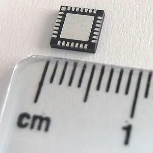
Figure 1. A quad flat no lead (QFN) package. QFNs are popular mid-range packages, which are used in various applications. They are small packages with good thermal performance. The image shows a 28-pin QFN, which is placed upside down to show the contacts and thermal/ground pads. Source: Wikipedia
Interposers vs bridges
The most advanced chips generally require a different package. For example, AMD, Nvidia and others have developed various AI chip architectures. Generally, an AI chip architecture requires an advanced package.
There are several different types of advanced packages in the market. One technology, called 2.5D, is a popular advanced package type for HPC applications.
2.5D can accommodate several dies, or chips, in the same package. In one 2.5D configuration, a processor die is placed on an interposer in the package. High bandwidth memory (HBM) is placed next to the processor on the same interposer. The silicon-based interposer is a structure with internal interconnects, which provides signals from the dies to the board.
HBM is a stack of DRAM dies, which are vertically connected using through-silicon vias (TSVs). HBM enables data to transfer between the processor and memory at high speeds.
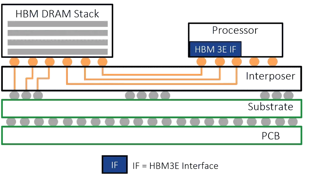
Figure 2. 2.5D package. An HBM stack and a processor die are situated on an interposer in the same package. Source: Rambus
For some time, 2.5D packages have been widely used for high-end applications, such as AI and HPC. But the problem is that the interposer is sometimes too expensive. The interposer also occupies too much unused real estate in the package.
“These interposers are currently the mainstream in HPC due to their ability to support the finest routing features, allowing for high-performance integration. However, the high costs of materials, high standard manufacturing, and limitations in the packaging area present challenges,” said Yu-Han Chang, a senior technology analyst at IDTechEx, in a recent report.
So, the industry is looking for new and alternative solutions. The silicon bridge is one possible solution to the problem.
For this solution, a company would still develop a 2.5D or related package type. But instead of using an interposer, the package makes use of a silicon bridge. As stated above, a bridge is a tiny piece of silicon, which connects one die to another in a package. Silicon bridges also have tiny routing layers, enabling electrical connections from one die to the next (See Figure 3 below).
“Localized Si bridges, which strategically use Si only where necessary, are gaining traction. This method helps overcome area limitations, especially beyond the 4x or 5x reticle limit,” Chang said.
Who are the bridge players?
Silicon bridge technology isn’t new. Back in 2017, Intel introduced a silicon bridge technology, dubbed Embedded Multi-die Interconnect Bridge (EMIB). EMIB is a cost-effective way to connect multiple and complex die in a package, according to Intel. Intel offers various advanced package types using EMIB.
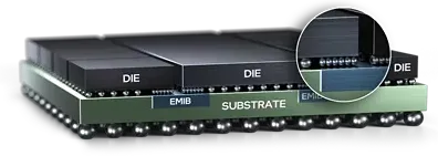
Figure 3. Intel’s Embedded Multi-die Interconnect Bridge (EMIB). Instead of an expensive silicon interposer, a small silicon bridge chip is embedded in the package, enabling high density die-to-die connections only where needed. Source: Intel
Meanwhile, in 2012, TSMC introduced its original 2.5D packaging technology, dubbed Chip-on-Wafer-on-Substrate (CoWoS). Basically, CoWoS can accommodate multiple dies in a 2.5D package. It makes use of an interposer. Today, TSMC calls it CoWoS-S.
Then, in 2022, TSMC introduced CoWoS-L. Like CoWoS-S, CoWoS-L is a 2.5D packaging technology. But instead of an interposer, TSMC is using a silicon bridge here.
CoWoS-L is gaining traction. For example, Nvidia is shipping Blackwell, a new GPU architecture designed for AI applications. This architecture combines a GPU device from Nvidia and eight HBMs in a 2.5D package. Nvidia is using TSMC’s CoWoS-L packaging technology for Blackwell.
Meanwhile, in 2023, ASE introduced a packaging technology called Fan-Out-Chip-on-Substrate-Bridge (FOCoS-Bridge). FOCoS-Bridge is positioned as an alternative to 2.5D packages using silicon interposers. Instead of using an interposer, ASE’s technology uses tiny silicon bridges.
Now, ASE has taken the technology to the next level by rolling out FOCoS-Bridge with TSV. In this product, the silicon bridge incorporates TSVs. The TSV bridge chips provide a shorter vertical path for power delivery in conjunction with traditional lateral signal connections.
The TSV and passive devices are embedded and interconnected using three redistribution layers (RDLs) with 5µm line and space. When compared to FOCoS-Bridge, the resistance and inductance of FOCoS-Bridge TSV are reduced by 72% and 50%, respectively, according to ASE.
ASE has demonstrated FOCoS-Bridge TSV using an 85mm x 85mm test vehicle comprised of two identical fan-out modules. Each module is made up of one ASIC chip and four HBM3 chips that are laterally interconnected with four TSV bridge chips as well as 10 integrated passive device chips.
“The growing demands of HPC and AI applications are accelerating the need for greater computational performance, and ASE’s FOCoS-Bridge capabilities enable seamless integration of SoCs and chiplets with high-bandwidth memory,” said Teck Lee, director of R&D at ASE. “By incorporating TSV, FOCoS-Bridge enhances compute and energy efficiency, and elevates our advanced packaging portfolio to the next level.”
And not to be outdone, IBM is expected to produce advanced packages based on Deca’s M-Series Fan-out Interposer Technology (MFIT). Deca’s MFIT solution includes embedded bridge dies, enabling a new class of multi-die packages.
Others also offer silicon bridges. For example, Amkor provides a bridge technology called Silicon Connect (S-Connect). In addition, Samsung Foundry offers a bridge technology called I-CubeE.