


IBM To Bring Deca’s Fan-Out Packaging Technology To North America
What is IBM doing in packaging and who are they working with?

By Mark LaPedus
IBM and Deca Technologies have formed a major alliance in the semiconductor packaging arena, a move that will enable IBM to enter the advanced fan-out wafer-level packaging market.
Under the plan, IBM is expected to establish a new high-volume manufacturing line in its existing packaging facility in Bromont, a city in southern Quebec, Canada. At some point in the future, IBM’s new manufacturing line is expected to produce advanced packages based on Deca’s M-Series Fan-out Interposer Technology (MFIT). MFIT enables a new class of complex multi-die packages.
Nonetheless, for years, IBM has provided packaging and testing services for outside customers, as well as for its internal needs, in Bromont. With the Deca announcement, IBM will expand its packaging capabilities and enter the fan-out wafer-level packaging (FOWLP) segment.
Basically, after a chip is manufactured in a fab, the device is then assembled into a package. A package is a small enclosure that protects a chip or multiple chips from harsh operating conditions. FOWLP is an advanced form of packaging, in which complex dies can be incorporated into a package. FOWLP and other types of packages can help boost the performance of a chip.
Deca’s MFIT is an advanced form of FOWLP, in which the latest memory devices, processors and other chips can be incorporated in a 2.5D/3D package. “MFIT is a high-density integration platform for AI and other memory-intensive computing applications,” said Tim Olson, chief executive of Deca. (See Figure 1 below).
Fan-out packaging is an enabling technology, but most, if not all, of the world’s FOWLP production capacity is located in Asia. ASE, TSMC and others produce fan-out packages in various locations throughout Asia.
Some customers, however, may want to have their chips manufactured, and then packaged, in North America. At some point, customers may have two new options for fan-out production capabilities in North America. IBM is working on it. In addition, SkyWater, a U.S.-based foundry vendor, is developing a fan-out production capability based on Deca’s technology in a facility in the U.S.
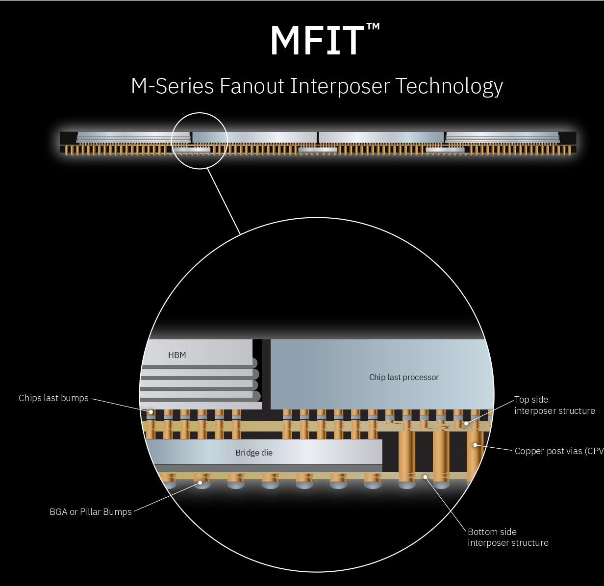
Figure 1. Deca’s MFIT solution offers dual sided routing, dense 3D interconnects, and embedded bridge dies for the heterogeneous integration of high bandwidth memory (HBM), processors and more. Source: Deca
(Very) brief history of IBM
IBM is an iconic brand in computing with a long history. It also has a long, and sometimes painful, history in the semiconductor industry.
The origins of IBM can be traced back to 1911, when an entity called the Computing-Tabulating-Recording Company (CTR) emerged. CTR supplied record-keeping and measuring systems. In 1924, CTR was renamed International Business Machines.
In 1952, IBM introduced its first business/scientific computer, dubbed the 701 Electronic Data Processing Machine. The 701 incorporated a trio of electronic devices--vacuum tubes, magnetic drums and magnetic tapes.
Four years later, IBM formed a new semiconductor R&D group. The goal was to find a replacement technology for outdated vacuum tubes for its systems. In the 1960s, IBM developed a new and more advanced replacement technology—solid-state electronics based on a newfangled technology called integrated circuits (ICs). Going forward, the company used more advanced chip technology for its computer lines.
Then, in 1966, IBM formed the Microelectronics Division, which became the company’s semiconductor arm. At that time, the company developed chips for its own systems. In the same year, IBM’s Robert Dennard invented the DRAM, a device that is still used for main memory in PCs, smartphones and other products.
Another major event took place in 1993, when IBM entered the merchant semiconductor market. The company manufactured and sold ASICs, processors and other chips to outside customers.
In the 1990s, IBM also entered the foundry business, setting the stage for a competitive battle against TSMC and others. For foundry customers, IBM provided leading-edge processes and RF technologies. It manufactured chips within its own fabs.
In the 2010s, though, IBM’s Microelectronics Division fell on hard times. The unit struggled in the merchant semiconductor business and lost millions of dollars in the arena. Its foundry business was also unsuccessful.
In 2014, IBM sold its Microelectronics Division, including the fabs and the foundry business, to GlobalFoundries (GF), a foundry vendor. IBM paid GF some $1.5 billion to take its Microelectronics Division.
IBM’s current semi/packaging efforts
Fast forward. Today, IBM is a provider of systems as well as hybrid cloud and consulting services. The company is still involved in the semiconductor industry. It designs processors and other chips, but it no longer manufactures them in its own fabs. It relies on foundry vendors to produce its chips.
In addition, IBM has a large semiconductor R&D center in New York. In 2015, the company’s R&D unit developed a breakthrough transistor technology called the nanosheet. Basically, the nanosheet is a next-generation gate-all-around (GAA) transistor.
Plus, for years, IBM has offered packaging and testing services for customers in Bromont. In fact, the Bromont plant is the largest outsourced semiconductor assembly and test (OSAT) facility in North America. In the facility, the company provides flip-chip assembly and testing services. It is also developing an assembly process for co-packaged optics.
IBM also has a major alliance with Rapidus, a foundry startup based in Japan. Rapidus is developing a 2nm process based on IBM’s nanosheet transistor technology.
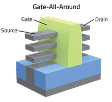
A nanosheet transistor structure. The nanosheet is a next-generation gate-all-around (GAA) transistor. Source: Lam Research
Rapidus and IBM are also co-developing various ways to produce chiplets. Basically, chiplets are small modular dies. The dies, or chiplets, are electrically connected and then combined in a package, creating a new and complex chip.
Now, with Deca, IBM is developing a fan-out packaging capability. According to IBM’s website, the company plans to add FOWLP manufacturing capabilities by the second half of 2026.
What is fan-out?
FOWLP isn’t new and technology has been around for some time. FOWLP gained notoriety in 2016, when Apple used TSMC’s fan-out packaging technology for its iPhone 7.
In the package, TSMC stacked a DRAM die on top of an application processor. The processor, called the A10, was designed by Apple and manufactured by TSMC using a 16nm process. Apple has also implemented TSMC’s fan-out packaging technology in subsequent phones.
FOWLP can be used in a variety of ways. For example, multiple dies and components, such as MEMS, filters, crystals and passives, can be incorporated in a fan-out package. But what makes fan-out unique is the ability to develop a small-sized package with a large number of I/Os.
In many cases, a small chip will reside in a large-sized package. That takes up too much space. In fan-out, the package “is roughly the same size as the die itself,” according to ASE. “Fan-out packaging can be defined as any package with connections fanned-out of the chip surface, enabling more external I/Os.”
Taiwan’s ASE, the world’s largest OSAT, produces a fan-out packaging line based on Deca’s M-Series technology. Nepes, a South Korean OSAT, is another licensee of Deca.
In R&D, IBM and SkyWater are working on fan-out based on Deca’s technology. Last year, SkyWater and Deca announced a $120 million contract with U.S. Department of Defense. By year’s end, SkyWater is expected produce fan-out packages in a U.S.-based facility.
Meanwhile, Deca itself has developed several different versions of its M-Series fan-out technology. In general, the M-Series enables customers to develop single- and multi-die packages, 3D packages and chiplets. For the M-Series, Deca has also developed a manufacturing technology called Adaptive Patterning, which is used to produce fine-pitch fan-out packages.
Deca’s M-Series includes one version called MFIT. This is an advanced technology, which includes dual-sided routing, dense 3D interconnects, and embedded bridge dies. It enables customers to develop multi-die packages that incorporate high bandwidth memory (HBM), processors and other devices.
“MFIT utilizes M-Series chips-first fan-out technology with embedded bridges to create a high-density interposer for chips last mounting of processors and memory chiplets. Adaptive Patterning allows a scaling roadmap to a very high density at a sub-10µm pitch,” Deca’s Olson said.
“MFIT uses Deca’s Gen 2 technology, which starts with a 20µm pitch for embedded components with a roadmap to finer pitches. Flip chip on the interposer for chips last devices initially mirrors the current industry leading pitches with a roadmap to finer pitches. Adaptive Patterning provides the ability to scale to finer pitches, while maintaining robust manufacturability through the design during the manufacturing process,” he said.
Fan-out isn’t the only option in the advanced packaging world. Other options include 2.5D and 3D packaging technologies as well as chiplets. All told, there are multiple options out there with more innovations to come.