


Corning Expands Glass Production For EUV Mask Substrates
The company has obtained CHIPS funding for its expansion plans. But the future is unclear for the CHIPS Act.

By Mark LaPedus
Corning has been awarded up to $32 million in funding under the CHIPS and Science Act to expand the production of its advanced glass products for use in etch, lithography and photomask applications.
The proposed investment in Corning would support the company’s expansion of its existing manufacturing facility in Canton, N.Y. The facility produces several products, including ultra-low expansion glass, which is used to develop the substrates for advanced photomasks. Photomasks or masks, sometimes called reticles, play an important role in extreme ultraviolet (EUV) lithography, a next-generation technology that helps produce today’s most advanced chips.
Corning, a supplier of specialty glass and other materials, is also known for its glass-based smartphone cover materials and other products.
Meanwhile, for years, the United States’ share of chip-manufacturing capacity has dwindled. In response, the U.S. government in 2022 launched a new program called the CHIPS and Science Act, which is designed to expand the production of chips in the United States. The other goal is to provide funding for various chip-manufacturing technologies, such as lithography, metrology and packaging.
There is some uncertainly with the CHIPS program, however. President-elect Donald Trump has been critical of the CHIPS Act, leaving many to wonder about the future of the program. For now, though, the CHIPS Act will remain in place. In a blog post, Counterpoint Research has provided an analysis of what the U.S. election means for the semiconductor industry and other sectors. Click here for the analysis.

Corning’s ultra-low expansion glass is a titania-silicate technology with near zero expansion characteristics. It has been tailored to meet the needs for the substrates used in EUV mask applications. Source: Corning
Mask/litho process
Nonetheless, lithography is one of several key technologies that is used to produce chips in a semiconductor manufacturing facility, typically called a fab. In a fab, a chipmaker (i.e. Intel, TSMC, Samsung) has a large installed base of systems called lithography scanners. Basically, a lithography scanner is a large and expensive system, which is used to create tiny and intricate patterns on chips. A chipmaker also has other types of equipment in the fab, enabling it to produce chips.
Lithography scanners can be split into two groups—optical and EUV. For years, optical-based lithography scanners were the most advanced systems used to pattern chips in semiconductor production. Optical lithography is still widely used today.
But starting around 2018, leading-edge chipmakers (i.e. Samsung and TSMC) migrated to a next-generation lithographic technology called EUV lithography. EUV is used to process the world’s most advanced chips at the 7nm process node and beyond.
One company, ASML of the Netherlands, is the sole supplier of EUV scanners in the market. Generating light with a wavelength of 13.5nm, EUV scanners incorporate a 0.33 numerical aperture (NA) lens with 13nm resolutions.
Soon, it will become too complicated to make chips using 0.33 NA EUV. So, ASML is developing a next-generation lithography system called high-numerical aperture (high-NA) EUV. Still in R&D, high-NA EUV scanners incorporate a different 0.55 NA lens with 8nm resolutions. ASML’s high-NA EUV scanners will enable chipmakers to print features 1.7 times smaller than today’s 0.33 NA EUV scanners.
Optical- and EUV-based lithography scanners are completely different systems. But both types require two common components to process chips, namely a photomask and wafer.
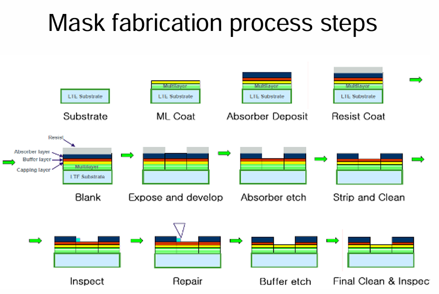
The first step in the lithographic process is to develop a photomask or mask. A mask, which measures 6- x 6-inches, is a component that serves as a master template of a unique chip design.
Source: Sematech
To make a photomask, the first step is to develop a mask blank. These components serve as the base material of a photomask. These components are made by mask blank vendors, such as AGC and Hoya.
Mask blanks for optical and EUV lithography are different. For optical lithography, the mask blank consists of light-shielding thin films on a synthetic quartz substrate.
In EUV, the blank consists of 40 to 50 alternating thin layers of silicon and molybdenum materials on a low-thermal expansion glass substrate. Corning develops these ultra-low expansion glass substrates and sells them to AGC and Hoya.
Once the mask blank is developed, this component is shipped to a photomask vendor. Then, using various equipment, a photomask vendor creates intricate patterns on the blank based on the specifications of a given chip design. This in turn creates a photomask.
The photomask is then shipped to a fab. In the fab, a chipmaker places the mask on a stage inside a lithography scanner. Then, a chipmaker places a 300mm round silicon wafer on a separate stage inside the same scanner.
In operation, a light source is generated inside the scanner, which is then projected through the mask. At that point, the mask patterns are projected onto a 300mm wafer.
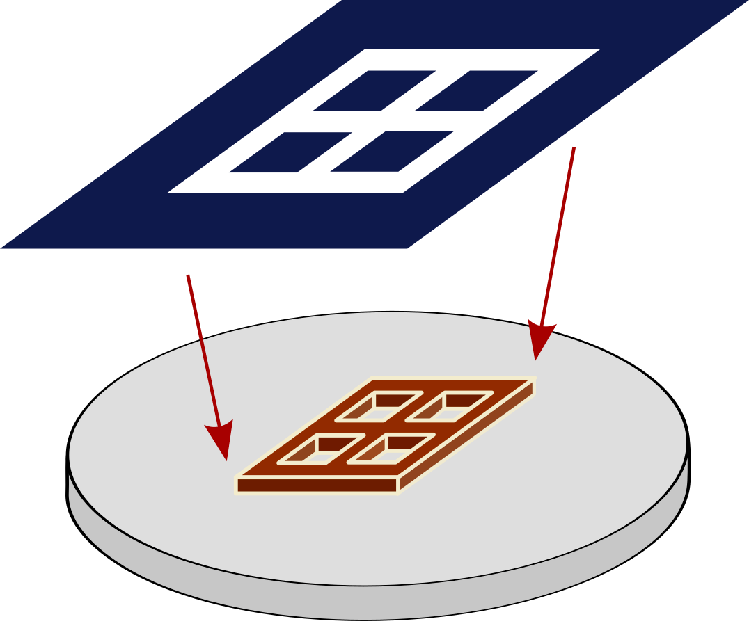
A schematic illustration of a photomask (top) and an IC layer printed using it (bottom). Source: Wikipedia
It’s not that simple. In the lithographic process, the goal is to develop and process anywhere from 200 to 400 separate chips, or dies, on each wafer. Let’s say the goal is to process 300 dies on a wafer. In this case, the scanner must create tiny patterns on 300 different and small square-like areas on the wafer. These square-like areas represent the chips, or dies, on the wafer.
To accomplish this challenging feat, the wafer on the stage is moved from one place to another in a precise location at high speeds. Then, the light from the scanner is projected to pattern an individual die at the nanometer scale. This process is repeated multiple times until all of the dies are processed. In the scanner, light is hitting the mask at temperatures of up to 500 degrees Celsius.
Amazingly, this process creates tiny and intricate patterns on each die on the wafer. The wafer is then subjected to other process steps in the fab. Eventually, finished dies, or chips, are created on the wafer. Finally, the dies on the wafer are diced, creating individual chips.
Low expansion glass
Nonetheless, the glass substrates from Corning play an important but overlooked part of the process. With funding from the CHIPS Act, Corning would enable a reliable domestic supply of these glass products in the U.S. In Corning’s Canton, N.Y.-based facility, the company plans to increase the production of its HPFS Fused Silica (High Purity Fused Silica) and EXTREME ULE Glass (Ultra Low Expansion Glass) products.
Corning’s HPFS Fused Silica is a glass product used for a range of applications. In the semiconductor world, the glass is used in etch equipment and other products. “Invented by Corning in the 1930s, this ultra-pure glass was used initially in radar technology and later in Space Shuttle windows and telescope mirrors,” according to officials from Corning. “Years later, this material and the process to produce it, chemical vapor deposition, was the starting point for the breakthrough in the optical communications revolution, and later for semiconductor manufacturing.”
In addition, Corning develops other products, including ULE, or ultra-low expansion glass. ULE is a titania-silicate glass technology that exhibits no dimensional changes over extreme temperature variations.
The thermal stability of Corning’s ULE glass makes it an ideal material for photomask substrates in EUV lithography applications. EUV lithography systems require a zero-expansion glass, due to the thermal loads produced on the optics during the exposure process.
In September of 2024, Corning unveiled EXTREME ULE Glass, a next-generation glass material for use in photomask substrate applications. Corning designed this glass to withstand highest-intensity EUV lithography, including high-NA EUV. The thermal expansion qualities of the glass help deliver consistency and performance across all photomasks. In addition, the flatness and uniformity reduce photomask waviness, helping limit unwanted variability.
“Corning EXTREME ULE Glass is ideal for EUVL photomask blanks. Corning EXTREME ULE Glass photomask blanks will provide a solution for >500W scanners as it provides tighter CTE uniformity and rotationally symmetric CTE profiles – significantly reducing striae and enabling improved flatness for photomask manufacturers,” according to officials from Corning.
“As the demands of integrated chipmaking grow with the rise of artificial intelligence, glass innovation is more important than ever,” said Claude Echahamian, vice president and general manager of Corning Advanced Optics. “EXTREME ULE Glass will expand Corning’s vital role in the ongoing pursuit of Moore’s Law by helping enable higher-powered EUV manufacturing as well as higher yield.”
Other news
Meanwhile, in addition to Corning, the U.S. Department of Commerce also awarded $3 million in funding to Powerex under the CHIPS Act. The proposed investment in Powerex would support the expansion of the company’s back-end production facility in Youngwood, Penn. This facility packages semiconductor power modules for defense applications, including the F-35, as well as commercial and industrial products.
On the photomask front, Toppan Photomask, a photomask provider, has changed its company name to Tekscend Photomask effective Nov. 1. In addition, Tekscend, in cooperation with The Advanced Mask Technology Center (AMTC) in Germany, has taken delivery and installed Europe’s first multibeam mask writer, the MBMW-100 Flex from IMS Nanofabrication.