


SK Hynix Surpasses Samsung in DRAM Share
Thanks to HBM, SK Hynix overtook Samsung for the first time in the worldwide DRAM market.

By Mark LaPedus
Thanks to a boom in the high bandwidth memory (HBM) market, SK Hynix has overtaken Samsung for the first time in the worldwide DRAM business in terms of market share, according to Counterpoint Research.
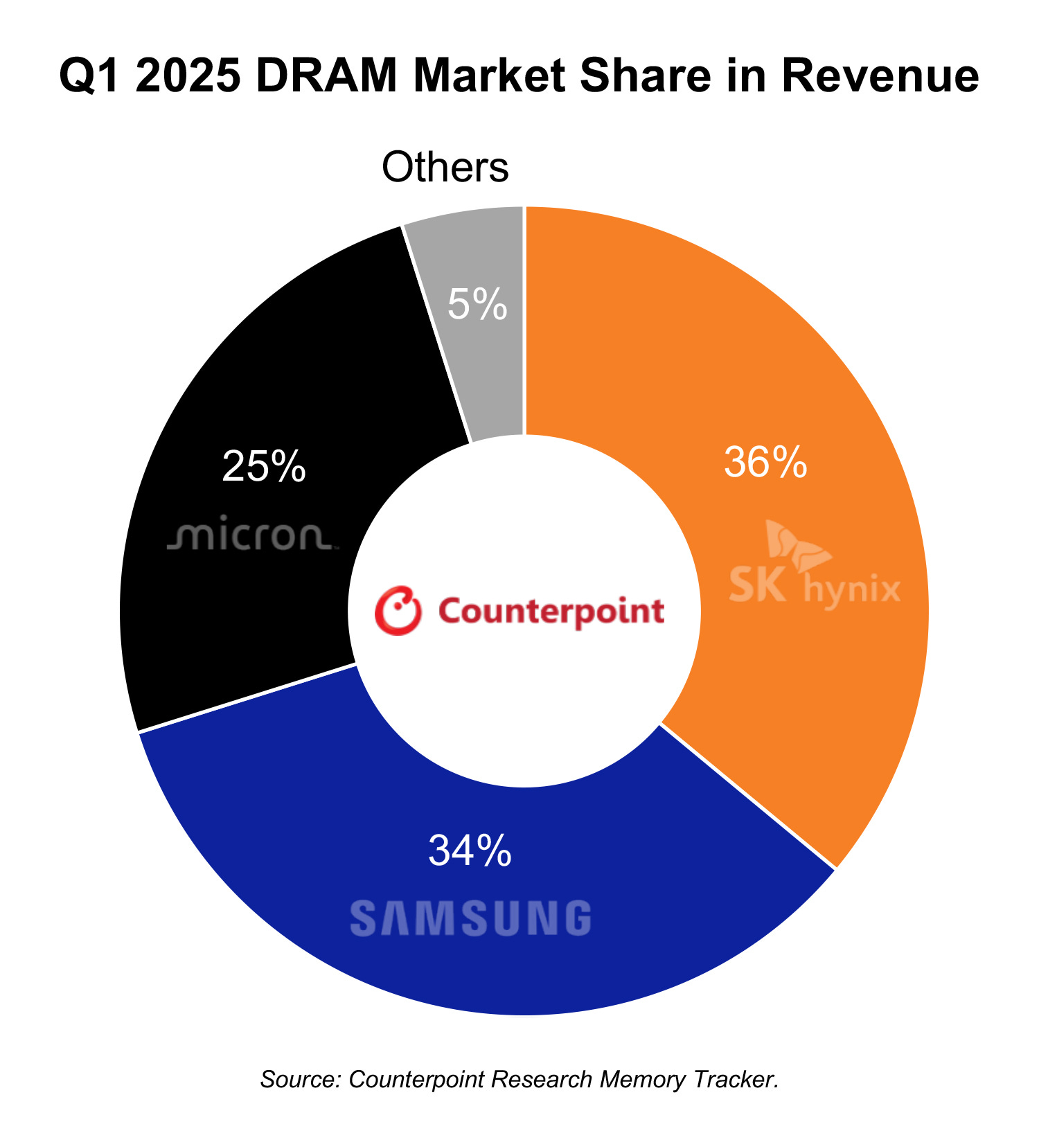
South Korea’s SK Hynix, which had been the world’s second largest DRAM maker for many years, took the lead for the first time ever in the DRAM market, grabbing 36% share of revenues in the first quarter of 2025, according to Counterpoint Research, a research firm.
South Korea’s Samsung, the long-time leader in the DRAM market, fell to second place with 34% share in the first quarter, according to the firm. U.S.-based Micron was in third place with 25% share. Other vendors had a total of 5% share.
“This is a milestone for SK Hynix which is successfully delivering on DRAM to a market that continues to show unfettered demand for HBM memory,” says Jeongku Choi, senior analyst at Counterpoint Research.
What is DRAM, HBM?
Computers and smartphones have the same basic architecture. A system incorporates a board. A central processing unit (CPU), memory and storage reside on the board. The CPU is a chip that processes the data. Systems also incorporate either a solid-state drive (SSD) or a hard disk drive. Both provide the data storage functions in systems.
A DRAM is a memory chip, which is widely used in cars, computers, smartphones and other products. DRAMs provide the main memory functions in systems.
For some time, the traditional DRAM market has been sluggish amid lackluster growth for PCs and smartphones. Micron, Samsung, SK Hynix and others make and sell DRAMs in the market. DRAMs are produced in large facilities called fabs.
In contrast, HBM is a hot market. HBM is a stack of DRAM dies that are electrically connected to each other. Thanks to the AI boom, HBM products are generally sold out in 2025 and possibly even 2026.
Micron, Samsung and SK Hynix are the main suppliers of HBM products. SK Hynix has dominated the HBM market with 70% market share, according to Counterpoint. Micron is a viable supplier, but the company lacks fab capacity for its overall HBM production.
Samsung continues to struggle in the HBM arena. That’s why SK Hynix leapfrogged Samsung in the overall DRAM market in the first quarter of 2025.
Generally, HBM is used in AI chip architectures from AMD, Nvidia and others. Demand for these AI chip architectures, particularly those from Nvidia, are enormous.
As stated, HBM is a stack of DRAM dies. To make an HBM product, a DRAM supplier takes a standard DRAM, and vertically stacks four, six, eight or twelve of these memory chips on top of each other. The DRAM dies are connected using tiny vertical wires called through-silicon vias (TSVs). The TSVs provide the electrical connections between each die.
Nvidia is a big driver for HBM. Today, Nvidia is ramping up Blackwell, a new GPU architecture designed for AI applications. This architecture combines a GPU device from Nvidia and eight HBMs all in the same 2.5D package.
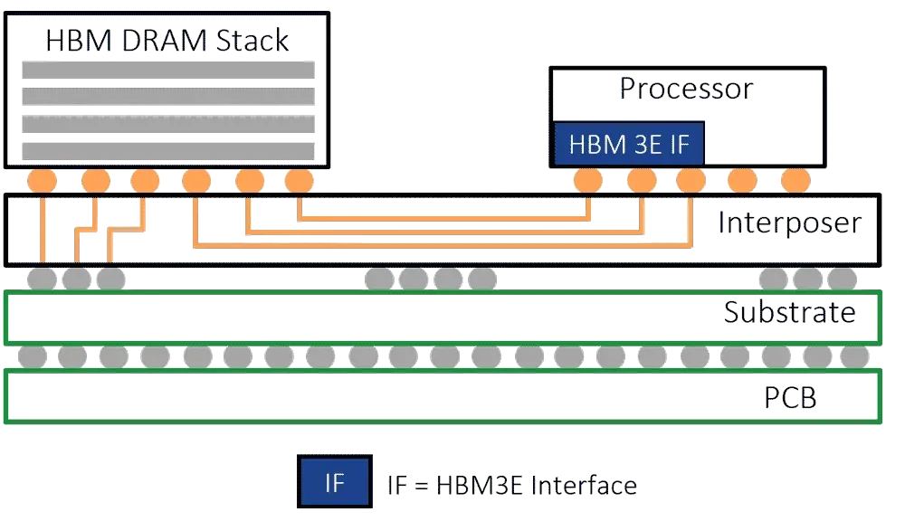
Here’s a 2.5D package. An HBM DRAM stack and a processor or GPU are situated on an interposer in the same package. In operation, the HBM enables the data to transfer between the memory and the processor or GPU at high speeds. Source: Rambus
In R&D, Nvidia is developing a new version of Blackwell, dubbed Blackwell Ultra, which is due out later this year. That AI architecture will also incorporate HBM devices.
In either case, HBM enables the data to transfer between the DRAM memory and the GPU at high speeds. HBM employs a 1024-bit memory bus, which is wider than standard DRAM. The wide bus enables high bandwidth in systems.
SK Hynix and Micron are the main suppliers of HBM for Nvidia. In 2025, HBM suppliers are ramping up HBM3E 12H products in the market. HBM3E is the latest standard for HBM products. 12H means that the HBM device stacks 12 DRAM dies.
For some time, Samsung has been trying to get qualified at Nvidia. But Samsung is struggling to meet spec at Nvidia due to yield issues.
Now, it appears that SK Hynix has encountered a slight glitch in HBM. “SK Hynix remains the primary supplier on Blackwell, but minor issues are resulting in MU being prioritized. SK has successfully been qualified on Blackwell Ultra with its HBM3E 12H memory and is expected to be the primary supplier to NVDA, also in part due to its greater capacity. However, we are hearing about minor performance issues with SK’s HBM memory that is causing NVDA to increasingly prioritize the use of MU’s HBM memory on Blackwell. However, the amount of share Micron is able to gain is obviously capped by its capacity, which we estimate at 4B-4.5B Gb this year,” said John Vinh, an analyst with KeyBanc Capital Markets, in a research note.
“Samsung (is) attempting to get qualified on Blackwell Ultra HBM3E 12H, but chances appear low. There is some optimism that Samsung may have a greater chance to get qualified on Blackwell Ultra with its HBM3E 12H memory as it uses a new design. However, we’re still hearing that it continues to struggle with thermal performance issues and is unlikely to be qualified for Blackwell Ultra,” Vinh said.
Now, Micron, SK Hynix and Samsung are racing each other to develop HBM products based on the next-generation HBM4 standard. There are several challenges to develop HBM4 products, which are due out in 2026 or perhaps earlier.
“The greatest challenge we will see is the rising complexity of HBM4 devices. HBM4 base logic wafers are being made at leading-edge logic foundries for use in high-performance data centers to power AI edge applications. This will make the supply chain more complex, and the requirements and manufacturing and testing processes for DRAM manufacturers, foundries, and SoCs will also become more complex as a result. So, more advancements will have to be made in test process optimization in the future to support the next generation of HBM,” said Jin Yokoyama, senior director and memory product marketing manager at Advantest, in a recent Q&A with Semiecosystem.