


A*STAR Launches Photonics Chiplet Consortium
Group hopes to address the challenges posed by integrating photonic chiplets in a package.

By Mark LaPedus
A*STAR’s Institute of Microelectronics (IME), a research and development organization in Singapore, has launched a photonics chiplet consortium.
The consortium, called the Advanced System-In-Package enabled by Heterogeneous Integration of HPC and Photonics Chiplets Consortium (CHIPLETS), includes the following companies: Asahi Kasei, Fujifilm, Rapidus, Toray Industries, Marvell, STATS ChipPAC and JCU.
The consortium is headed by IME, a research institute under Singapore’s Agency for Science, Technology and Research (A*STAR). IME is involved with several R&D projects, including advanced packaging, MEMS, silicon carbide (SiC), gallium nitride (GaN), photonics and sensors.
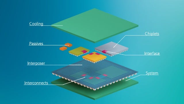
IME and many others are also pursuing chiplets, which are becoming an important part of the semiconductor industry. Today’s AI chips, processors and other high-performance devices are fast and highly-integrated devices. These chips are also relatively large, and are difficult and expensive to manufacture in the fab.
One way to solve these problems is to embrace the chiplets concept. In chiplets, the idea is to break up a large device into smaller dies. Then, the dies are assembled in an advanced package. A package is a product that encapsulates a chip, protecting it from harsh operating conditions.
There are several challenges to implement a chiplet-based design. A number of companies and R&D organizations are addressing those challenges. For example, Fraunhofer, a German R&D organization, has launched a new R&D center to propel the development of chiplets for the automotive industry.
Electronics solutions based on chiplets are the first to allow the integration of various functional units in different technologies on a substrate or into a 3D chip structure. © Fraunhofer IIS/EAS
There is also a wave of activity for chiplets in the silicon photonics world. “Photonics is similar to electronics. However, instead of electrons, it uses photons to transfer information,” according to a blog from PhotonDelta, a photonics technology accelerator in the Netherlands.
Over the years, several companies and R&D organizations have developed photonic integrated circuits (PICs), which work by using photons, or particles of light, to transfer, sense, process, and transmit information. “Using waveguides to control and direct light through total internal reflection, photonic integrated circuits are comparable to the wires used to carry electrical signals. A laser source provides the light needed to drive the components, similar to a switch in an electrical circuit,” according to PhotonDelta.
Photonics isn’t new and has been used in a number of fields, including augmented/virtual reality (AR/VR) systems, displays, renewable energy sources, and data communications.
Photonics is seen as a major enabler in the data center. In 2024, the world is expected to generate 1.5 times the digital data as compared to 2022, according to KKR, a global investment fund.
In many cases, the data is processed and distributed in large facilities called data centers. A large-scale facility, called a hyperscale data center, is a building that contains at least 5,000 servers and occupies 10,000 square feet of physical space, according to IBM. A single facility draws over 100 megawatts of power.
That’s just one facility. Amazon, Google, Meta, Microsoft and others own and operate a number of data centers throughout the world. These companies are referred to as cloud service providers (CSPs).
Meanwhile, a server, or computer, comes in different sizes and configurations. Each server consists of several chips, such as processors, GPUs and memory. A server also has a power supply, cooling fans and network switches.
In a data center, CSPs tend to incorporate multiple servers in a single rack or cabinet. The most common server rack size is 42U, which accommodates 42 servers in the same rack, according to Data Center Knowledge, a news and analysis site.
The servers in each rack must communicate with each other at high speeds. Then, the systems must communicate to other servers in different racks in a complex network.
That’s a major challenge. Up to 76% of all data center traffic traverses inside the data center itself, according to Tony Chan Carusone, a professor of electrical and computer engineering at the University of Toronto and chief technology officer at Alphawave Semi, in a video.
At one time, the servers in a rack communicated with each other using copper cables. Then, a system called a switch routes data to other racks using Ethernet links. Generally, though, optical fiber is displacing copper cables for shorter-reach applications in many data centers. Optical fiber, which is faster than copper, is used to connect the servers in a rack, as well as to other racks.
For optical networks, you need to convert electrical signals from the chips on the board into optical signals and vice versa. To accomplish this task, the data center generally uses a product called a pluggable optical transceiver. A pluggable optical transceiver is a small module, which resides next to the board. “Pluggable optics are interchangeable transceiver modules that connect different network components, such as switches, routers, and servers, to convert high-speed electrical signals into optical signals and vice versa,” according to Ayar Labs, an optical chiplet vendor.
Pluggable transceiver modules, however, have some limitations in data centers, especially for systems using GPUs in AI applications. “Currently, these systems rely on pluggable optical connections, which are essentially optical networking technology. Pluggables are great for long-haul applications, like telecommunications, but not designed for on-board input/output,” said Vladimir Stojanovic, chief architect and co-founder of Ayar Labs, in a blog. “Pluggables fail for GPU I/O in all four categories: bandwidth/latency, power, density, and cost.”
In response, companies are developing different solutions, including co-packaged optics (CPO), in-package optical I/O and others. Basically, instead of using external pluggable modules, the goal is to integrate the PICs next to the GPU or processor on the board. The PICs, along with the GPUs or processors, could even reside in the same IC package.
CPO is a way to integrate the optics and silicon on a single packaged substrate. Broadcom, Cisco and others are developing CPO solutions.
Ayar, Intel and others are developing in-package optical I/O technology. In one example of this technology, an ASIC and four optical transceiver chiplets are placed in the same IC package. Two of the chiplets reside on one side of the ASIC, while two other chiplets reside on the other side.
It also requires a separate external laser source module. This small laser module incorporates continuous wave lasers. This unit provides the optical power over fiber to the chiplets inside the package. The optical chiplets, in turn, convert electrical signals from the chips on the board into optical signals and vice versa.
All told, in-package optical I/O technology is faster than traditional pluggable modules. For example, Ayar Lab’s optical I/O chiplet enables 16 Tbps of bi-directional bandwidth. Compliant with the CW-WDM MSA specification, the 16-wavelength light source can supply light for 256 data channels.
“In-package optical I/O enables both high bandwidth and a high number of ports (links) out of the compute/switch package, providing flexibility in how the fabric is configured to meet evolving model requirements. For example, the system design could emphasize higher radix (more links), enabling growth in the number of nodes as necessary to support larger model tensor parallelism at lower latencies. Alternatively, it could emphasize higher throughput per link to enable lower transfer latencies with pipelined parallelism,” Stojanovic said.
Still, pluggable transceivers dominate the data center landscape. And there are challenges to implement CPO and in-package optical I/O. It’s expensive and difficult to integrate optics in a package.
The new optical chiplet consortium from A*STAR hopes to address these and other issues. “With the rise of Generative AI, the need for faster, more efficient computing is greater than ever. Our consortium aims to create a cutting-edge heterogeneous integration platform that integrates compute, memory, and optical I/O chiplets from various technologies. This innovative approach overcomes the limitations of traditional system-on-chip (SoC) designs, delivering smaller, more powerful packages that boost efficiency in power, performance, and cost—perfect for AI applications with high compute needs,” according to A*STAR.